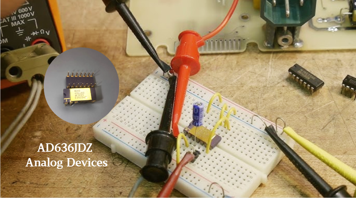
The Analog Devices AD636JDZ is a high - performance RMS - to - DC converter. It enables accurate conversion of various waveforms into equivalent DC values, handling inputs from 0 mV to 200 mVrms. With low - noise operation, fast response, and versatile power supply options (dual or single - supply), it suits diverse applications. Integrated with a buffer amplifier and featuring a dB output, it comes in a compact 14 - pin SBDIP package, ideal for space - limited circuits.
Analog Devices AD636JDZ's Features
- Accurate Conversion: It offers precise true - RMS to DC conversion, ensuring accurate measurement of various input waveforms, including complex and non - sinusoidal signals.
- Wide Input Range: The device can handle input signals from 0 mV to 200 mVrms continuously, and tolerate peak transient inputs up to ±2.8 Vp - p depending on the power supply, accommodating a variety of signal levels.
- Low Noise: It has low - noise performance, which is crucial for obtaining accurate measurement results, especially when dealing with weak input signals.
- Fast Response: The AD636JDZ features a relatively fast response time, allowing it to quickly track changes in the input signal and provide timely RMS - to - DC conversion.
- Versatile Power Supply: It can operate from dual - supply voltages ranging from ±2.5 V to ±16.5 V or a single - supply voltage from +5 V to +24 V, offering flexibility in different circuit designs.
- Integrated Buffer Amplifier: The chip incorporates a buffer amplifier, providing high - impedance input and low - impedance output, which helps minimize signal - source loading and simplifies interfacing with other components.
- dB Output Capability: In addition to the RMS - to - DC conversion, it provides a dB output pin with an externally settable 0 dB reference level, facilitating the convenient measurement and representation of signal levels in decibels.
- Compact Package: Housed in a 14 - pin SBDIP, it has a small footprint, making it suitable for space - constrained printed - circuit - board designs.
Analog Devices AD636JDZ's Applications
The AD636JDZ is a low-power, high-precision true RMS-to-DC converter that finds wide applications in various circuit scenarios, mainly including the following aspects:
General Measurement Applications
Standard Connection Measurement: In most high-precision root mean square (RMS) measurement scenarios, the connection method is simple. Only an external capacitor is required to set the average time constant. It can measure the RMS values of the AC and DC levels in the input signal. However, for low-frequency inputs, errors will occur due to the filter capacitor CAV, while the measurement accuracy meets the specifications for high-frequency inputs. For example, when using a 4μF capacitor, the additional average error for a 10Hz input signal is 0.1%, and it is 1% at 3Hz. If the DC input needs to be removed, a non-polar capacitor can be connected in series at the input. If there is high-frequency ripple in the power supply, a 0.1μF ceramic disc capacitor should be used to bypass the power supply to the ground, and an optional output ripple filter CF can also be added.
Optional High-Precision Trimming: If higher precision is pursued, an external trimming circuit can be added. Adjust the output offset through R4, adjust the scale factor using R1, and inserting R2 can make the adjustment range of R1 for the scale factor reach ±1.5%. When trimming, first ground the input and adjust R4 to make the output 0V. Then connect the full-scale input signal (DC or a 1kHz calibrated AC signal), and adjust R1 to make the output correct.
Power Supply Related Applications
Single-Power-Supply Connection and Use: Generally, the application assumes the use of a dual-power supply. However, by connecting three external biasing components to the COM pin, the AD636JDZ can use a unipolar power supply as low as 5V. The external bias voltage is reflected internally to the VIN pin, enabling AC operation similar to that of a dual-power supply. But the DC or AC + DC conversion is less practical due to the offset of the input DC level. In addition, the COM pin of some CMOS ADCs can serve as an artificial ground for the AD636JDZ. For AC input coupling, only one capacitor is required.
Signal Processing Applications
Selecting the Average Time Constant to Optimize the Output: The AD636JDZ can calculate the RMS values of AC and DC signals. When the input is a slowly changing DC voltage, the output can accurately track it. At high frequencies, the output approaches the RMS value of the input signal, but there are DC errors and ripples. The minimum value of CAV that meets the DC error requirements for a specific frequency can be determined according to Figure 13. Reducing the ripple can be achieved by increasing CAV, but it will increase the settling time when there is a step change in the input level. A better method is to use a post-filter. A single-pole filter (removing C3, shorting Rx, and making C2 approximately 5 times CAV) can reduce the ripple but will increase the settling time. A dual-pole post-filter can further reduce the ripple without significantly increasing the settling time. However, when selecting CAV, caution is required because it affects the DC error and is independent of the post-filter.
Specific Measuring Instrument Applications
Design of an AC Digital Voltmeter: A complete low-power AC digital voltmeter circuit can be constructed. A 10MΩ input attenuator is used to achieve full-scale measurement ranges of 200mV, 2V, 20V, and 200Vrms. The signal is capacitively coupled to the buffer amplifier of the AD636 (using an AC bootstrap configuration to reduce the load effect), and then drives the 6.7kΩ input impedance of the AD636. The COM terminal of the ADC provides a virtual ground for single-power-supply operation. In the linear RMS mode, a 1.2V reference diode AD589 provides a stable 100mV reference voltage for the ADC. In the dB mode, a 1N4148 diode is connected in series to correct the temperature coefficient of the dB scale factor. Adjust R13 to calibrate the full-scale reading, and adjust R9 and R14 to calibrate the 0dB reference point and the scale factor of the dB range respectively. When using a type 7106 ADC, the total power supply current of the circuit is usually 2.8mA.
Construction of a Low-Power High-Impedance dB Meter: A portable dB meter circuit can be formed, integrating the RMS conversion function of the AD636JDZ, the AD589 voltage reference, and the μA776 low-power operational amplifier. The built-in buffer amplifier of the AD636 is used as a bootstrap input stage, increasing the input impedance to approximately 1010Ω. The input voltage is AC-coupled through C4, and R8, D1, and D2 provide high input voltage protection. The output of the buffer is coupled to the input of the RMS converter through C2. R9 is connected between the output of the buffer and the negative output swing, and R1 is the bootstrap resistor. The ground potential is set through a specific resistor network to achieve single-power-supply operation. The AD589 establishes a regulated 1.2V reference voltage, and together with R3 and the potentiometer R4, it sets the 0dB reference current IREF. The 0dB reference range of this dB meter is from 0dBm (770mV) to -20dBm (77mV) rms, the input range (when IREF=770mV) is 50dBm, the input impedance is approximately 1010Ω, the power supply operating range is +5Vdc to +20Vdc, the typical value of the quiescent current is 1.8mA, and it has different accuracies within different dBm ranges, and the frequency response has corresponding ranges at different input dBm levels. The calibration includes calibrating the 0dB reference level (applying a 1kHz sine wave and adjusting the IREF calibration trimmer to make the analog meter indicate zero) and calibrating the meter scale factor or gain (applying an input signal 40dB lower than the set 0dB reference and adjusting the scale factor calibration trimmer to make the analog meter read 40μA). The temperature compensation resistors can be purchased from the specified suppliers.
Analog Devices AD636JDZ's Attributes
| Package |
Tube |
Product Status |
Active |
| Current - Supply |
800 µA |
Voltage - Supply |
±2.5V ~ 16V |
| Mounting Type |
Through Hole |
Package / Case |
14-CDIP (0.300", 7.62mm) |
| Supplier Device Package |
14-CDIP |
Base Product Number |
AD636 |

Analog Devices AD636JDZ's CAD Model
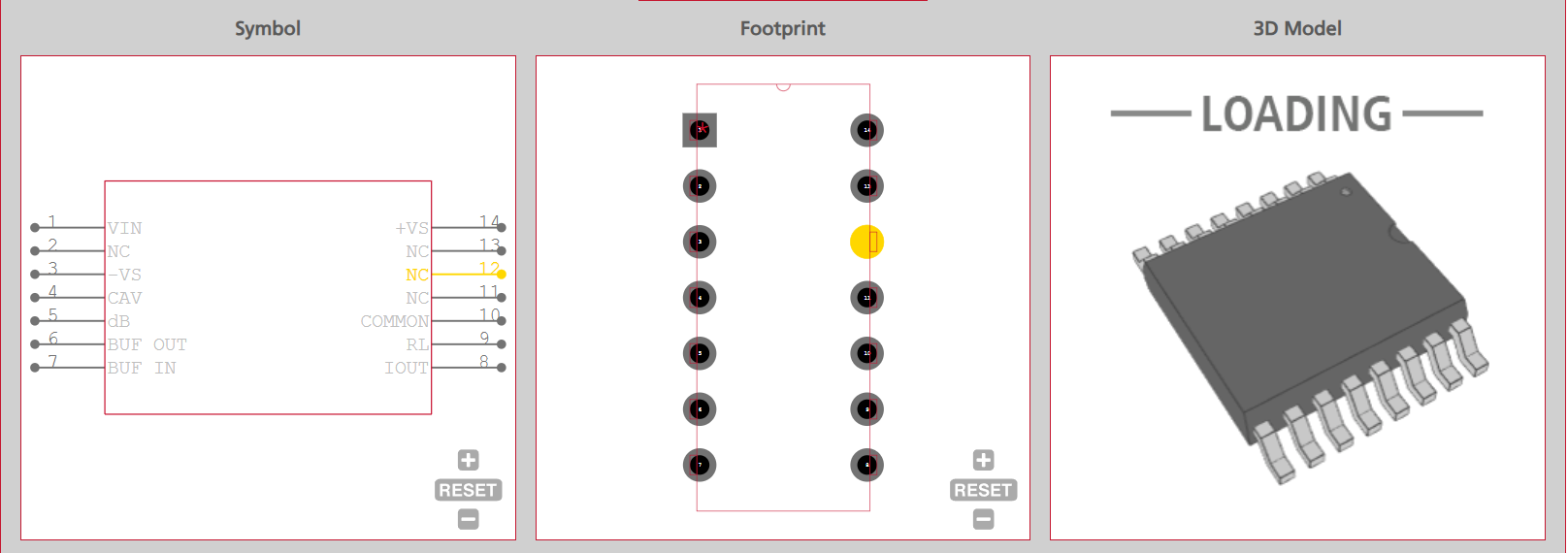
Analog Devices AD636JDZ's Pinouts
The AD636JDZ is packaged in a 14-pin SBDIP (Side-Brazed Ceramic Dual In-Line Package), and each pin has a clear function, playing a crucial role in circuit connection and signal processing.
Power Supply Pins
- Positive Power Supply Pin (+VS, Pin 14): It provides positive power input for the chip. The supply voltage range is ±2.5V to ±16.5V in the dual-power supply mode and +5V to +24V in the single-power supply mode. When the chip is operating normally, an appropriate positive power supply needs to be connected to ensure that the internal circuit can obtain the required electrical energy and maintain the normal operation of each functional module.
- Negative Power Supply Pin (-VS, Pin 3): In a dual-power supply system, it works in conjunction with the positive power supply pin to provide a complete power loop for the chip. In specific application scenarios, such as some circuits that require precise processing of positive and negative signals, the negative power supply can ensure the processing accuracy and stability of the chip for signals.
Signal Input Pin
- Signal Input Pin (VIN, Pin 1): It is used to connect the input signal that needs to undergo true RMS-DC conversion. This signal can be an AC signal, a DC signal, or a mixed AC-DC signal. The input signal range is 0mV to 200mVrms (continuous RMS level), and it can withstand certain transient inputs. For example, when powered by ±3V or -5V power supplies, the peak transient input is ±2.8Vp-p.
Function-related Pins
- Average Capacitance Pin (CAV, Pin 4): An external average capacitance is connected. This capacitor, together with the internal circuit of the chip, determines the average time constant of the signal, which has an important impact on the measurement accuracy and the stability of the output signal. When measuring signals of different frequencies and characteristics, an appropriate average capacitance value needs to be selected according to actual needs to balance the low-frequency accuracy, ripple, and stabilization time.
- dB Output Pin (dB, Pin 5): It outputs a signal representing the logarithmic value of the RMS output voltage. The 0dB reference level can be set by the externally provided current, and the setting range corresponds to the input level from 0dBm (774.6mV) to -20dBm (77.46mV). In some application scenarios where the signal power or amplitude is represented logarithmically, such as the measurement of communication signal strength, the signal output from this pin can be directly used for subsequent signal processing and display.
- Buffer Output Pin (BUF OUT, Pin 6): As the output terminal of the buffer amplifier, when an external load is connected to the chip, the buffered and amplified signal can be obtained from this pin. It has a strong output current capability and can output up to 5mA of current, which can drive some loads that require a large driving current, such as the input stage of certain types of ADCs.
- Buffer Input Pin (BUF IN, Pin 7): It is the input terminal of the buffer amplifier and is used to connect the signal that needs buffer processing. In some applications, the input signal can be connected to this pin first, and the buffer amplifier inside the chip can be used to increase the input impedance and reduce the loss and interference during signal transmission.
- RMS Output Current Pin (IOUT, Pin 8): It outputs a current signal corresponding to the RMS value of the input signal. The nominal ratio of the output current is 100μA of output current corresponding to every 1Vrms of input. In practical applications, the current signal can be converted into a voltage signal according to this characteristic for measurement or subsequent processing.
- Load Resistance Pin (RL, Pin 9): A load resistance is connected. The size of the load resistance will affect the output characteristics and performance of the chip. When designing the circuit, an appropriate load resistance value needs to be selected according to specific application requirements and the electrical parameters of the chip to ensure that the chip can work stably and accurately.
- Common Pin (COM, Pin 10): As the common reference point of the circuit, when powered by a single power supply, the chip can work normally by connecting an external bias circuit; when powered by a dual power supply, it provides a unified reference potential for each signal to ensure the accuracy and stability of signal processing.
- Unconnected Pins (NC, Pins 2, 11, 12, 13): These pins are not connected to any functional circuit inside the chip. When using the chip, they are usually not connected or processed to avoid abnormal operation of the chip caused by misconnection.
Analog Devices AD636JDZ's Category-RMS to DC Converters
RMS to DC converters play a pivotal role in the realm of electrical measurement and signal processing. They are designed to convert the root - mean - square (RMS) value of an alternating current (AC) or complex waveform into an equivalent direct current (DC) value. This conversion is essential as the RMS value represents the effective power - delivering capability of an AC signal, comparable to a DC voltage or current of the same value in terms of power dissipation in a resistive load. RMS to DC converters find applications in diverse fields, including power measurement in electrical systems, audio engineering for signal - level monitoring, and telecommunications for analyzing signal strengths.
Among the many RMS to DC converters available, the Analog Devices AD636JDZ stands out as a high - performance option. It offers accurate RMS to DC conversion, handling a wide input signal range from 0 mV to 200 mVrms. With its low - noise operation, high - speed response, and versatile power - supply options, it can be integrated into various electronic systems seamlessly. The integrated buffer amplifier and dB output capability further enhance its functionality, making the AD636JDZ an ideal choice for demanding measurement and signal - processing applications.
AD636JDZ's Manufacturer-Analog Devices
Analog Devices (ADI) has made remarkable achievements in the field of RMS - to - DC Converters. These converters are widely used in applications where precise low - power measurement of AC signals is crucial. ADI's RMS - to - DC converters are capable of providing real - time measurements, eliminating delays that limit the frequency response of other technologies. They can accurately measure complex waveforms, not just sine waves, over a wide input frequency range, with the DC output corresponding precisely to the RMS input. For example, the AD8436, a precision monolithic true RMS - to - DC converter, offers a best - in - class dynamic range from 100 µV to 3 V. It can measure extremely low signal levels with high accuracy, and its AC conversion accuracy is better than ±0.5%. Moreover, it extends the crest - factor to 10, approximately double the current industry - standard digital solution, while maintaining minimal loss of accuracy. ADI also provides a diverse range of RMS - to - DC converters. These converters are optimized for applications with strict requirements for performance, power consumption, and cost, effectively meeting the true RMS needs of various industries. Their contributions have significantly advanced the development of AC signal measurement technology.
AD636JDZ vs AD620AR
| Pictures |
 |
 |
| Part number |
AD636JDZ +BOM |
AD620AR +BOM |
| Manufacturer |
Analog Devices, Inc |
Analog Devices |
| Package |
CDIP-14 |
SOIC-8 |
| Description |
This converter operates at a frequency of up to 1500kHz |
Available in 8-pin SOIC package |
| Stock |
2789 |
4132 |
| RoHS |
True |
N |
| Series |
AD636 |
AD620 |
| Mounting Style |
Through Hole |
SMD/SMT |
| Minimum Operating Temperature (°C) |
0 |
- 40 |
| Maximum Operating Temperature (°C) |
+ 70 |
+ 85 |
| Collector-Emitter Saturation Voltage |
- 5 V to 3 V |
+/- 2.3 V to +/- 18 V |
| Product Type |
Power Management Specialized - PMIC |
Instrumentation Amplifiers |
| Factory Pack Quantity |
25 |
98 |
| Unit Weight |
0.325120 oz |
0.019048 oz |
| Manufacturer Type |
Converters |
|
| MAX Output Current |
130 uA, 5 mA |
|
| Input Voltage Range |
- 5 V to 3 V |
|
| Output Voltage Range |
0 V to 1 V |
|
| High Level Output Current |
1 mA |
|
| Collector- Emitter Voltage VCEO Max |
3 V |
|
| Input Voltage, Min |
- 5 V |
|
| Maximum Output Voltage |
1 V |
|
| Current @ Pmpp |
1 mA |
|
| Number of Channels |
|
1 Channel |
| 3 dB Bandwidth |
|
1 MHz |
| CMRR - Common Mode Rejection Ratio |
|
73 dB |
| Current - Input Bias |
|
2 nA |
| Vos - Input Offset Voltage |
|
125 uV |
| Amplifier Type |
|
Instrumentation Amplifier |
| Dual Supply Voltage |
|
+/- 2.3 V to +/- 18 V |
| Height |
|
1.5 mm (Max) |
| Length |
|
5 mm (Max) |
| Maximum Dual Supply Voltage |
|
+/- 18 V |
| Maximum Input Resistance |
|
10 GOhms (Typ) |
| Minimum Dual Supply Voltage |
|
+/- 2.3 V |
| Pd - Power Dissipation |
|
650 mW |
| Product |
|
Instrumentation Amplifiers |
| Supply Type |
|
Dual |
| Width |
|
4 mm (Max) |
WlS Electronic holds a large inventory of AD636JDZ from Analog Devices. We assure you that these are genuine and brand - new components, directly sourced from Analog Devices. If needed, we can provide quality test reports for the AD636JDZ. To obtain a quotation, simply fill in the desired quantity, your contact name, and your email address in the quick quotation form on the right. Our sales representatives will get in touch with you within 12 hours. You can contact us online at any time, or send an email to: SALES@WLSCHIP.COM.


