The TL494 is a classic Pulse Width Modulation (PWM) controller IC introduced by Texas Instruments (TI). It integrates dual error amplifiers, an adjustable oscillator, a PWM comparator, and push-pull/single-ended output driver circuits, specifically designed for switch-mode power supply control. Its core features include a 5V reference power supply, adjustable dead-time control (0–100%), cycle-by-cycle overcurrent protection, support for setting up to 300kHz switching frequency via RT/CT pins, and multi-chip synchronization through external signals. The IC can be configured for voltage/current dual-loop control, suitable for topologies like flyback, forward, and half-bridge, and is widely used in ATX power supplies, battery chargers, and industrial DC-DC conversion. With its low cost, high integration, and flexible topology adaptability, the TL494 has become a classic solution for medium-low power (<200W) power supply systems, offering both commercial grade (0°C–70°C) and industrial grade (−40°C–85°C) temperature versions.
TL494 Features
I. Core Architecture of Current-Mode Control
Dual Error Amplifiers (Voltage + Current Dual Loop)
Error Amplifier 1 (1IN±/2IN±): Main voltage loop samples output voltage and controls PWM duty cycle via PI regulation.
Error Amplifier 2 (2IN±/FEEDBACK pin): Current loop directly samples switch current (e.g., MOSFET source resistor voltage drop or hall sensor signal) to achieve cycle-by-cycle current limiting.
Dual-loop Collaboration: The current loop responds in microsecond-level to suppress input voltage fluctuations and load transients, while the voltage loop ensures long-term steady-state regulation. Typical applications include double-ended forward and half-bridge topologies requiring current balancing (Summaries 4, 6).
Current Sensing Interface (FEEDBACK Pin, Pin 3)
Supports direct connection of current sensing signals (e.g., 0.1Ω sensing resistor). The error amplifier 2 compares the signal with the internal sawtooth wave to adjust duty cycle in real time.
Example: In a 5V/10A power supply, a 0.1Ω resistor samples current. When overcurrent occurs, the voltage at Pin 3 rises, forcing pulse width reduction (Summaries 3, 4).
Cycle-by-Cycle Overcurrent Protection (OCP)
The current loop has higher priority than the voltage loop. Upon detecting overcurrent (e.g., short circuit), it blocks outputs immediately with a response time < 1 switching cycle (Document Section 9.3.6).
II. Exclusive Features of Current-Mode Control
Automatic Current Sharing (Push-Pull/Half-Bridge Topologies)
In push-pull mode (Pin 13 connected to REF), dual outputs drive alternately, and the current loop ensures current balance between two switches to avoid flux bias (double-ended forward design in Summary 4).
In single-ended parallel mode (Pin 13 grounded), dual outputs drive synchronously, suitable for high-current scenarios (e.g., 10A power supply, Summary 3).
Wide-Range Current Detection (-0.3V to Vcc-2V Common-Mode Input)
The error amplifier's common-mode range includes negative voltages, allowing low-side current sensing (e.g., switch source grounded with a sensing resistor at the source), reducing high-voltage isolation requirements (Document Section 7.7).
Decoupling of Dead Time and Current Control
Dead time is independently adjusted by Pin 4 (DTC) (0~3.3V corresponding to 3%~100% dead time), not affecting current loop dynamic response and avoiding switch shoot-through (dead time control analysis in Summary 5).
III. Typical Current-Mode Application Scenarios
Double-Ended Forward Power Supply (e.g., 5V/10A Design)
A hall sensor samples primary current, forming a current loop via Error Amplifier 2. Combined with the voltage loop, it achieves constant voltage/constant current (CV/CC) dual modes (Summary 4).
Reduced switch voltage rating (only 2× input voltage), suitable for medium-low power industrial supplies.
Flyback Fast Charging (Requiring Constant Current Charging)
Secondary current is fed back to Error Amplifier 2 via an optocoupler to enable precise control during constant current charging (load regulation mentioned in Summaries 2, 6).
Multi-Phase Parallel Current Sharing
Multiple TL494s are synchronized, sharing current sensing signals to achieve current sharing across phases, enhancing system power density (Document Section 10.2 typical application).
IV. Limitations and Compensation Design
Ramp Compensation Requirement
Current mode is prone to oscillation when duty cycle > 50%. Ramp compensation must be injected via Pin 4 (DTC) (e.g., series RC to sawtooth wave) for stability (0.12V dead time offset mentioned in Summary 5).
Switching Frequency Limitation
Maximum switching frequency of 300kHz (Document Section 7.3), suitable for low-to-medium frequency current sensing (e.g., BJT driving). MOSFET driving requires optimized driver circuits (additional driver circuit mentioned in Summary 1).
Summary: Core Advantages of TL494 Current-Mode Control
| Feature |
Description |
| Dual-loop Control |
Voltage loop (steady state) + current loop (transient), response <1μs, ideal for dynamic loads. |
| Cycle-by-Cycle Protection |
Direct switch current detection enables high-precision short-circuit protection (e.g., 0.1Ω sensing in 10A supply, Summary 4). |
| Topology Adaptability |
Supports push-pull/half-bridge/forward topologies with automatic current sharing, reducing transformer flux bias risk. |
| Low-Cost Solution |
Integrated error amplifiers and reference eliminate the need for extra current control ICs, suitable for medium-low power (<200W). |
TL494 Applications
I. Consumer Electronics and Computer Power Supplies
- ATX Power Supplies (PC Switching Power Supplies)
- Topology: Half-bridge/dual-transistor forward + synchronous rectification
- Functions:
- Dual error amplifiers implement voltage loops (12V/5V output regulation) and current loops (phase current sharing) to meet CPU dynamic load requirements.
- Push-pull mode drives primary-side switching transistors, with dead-time control preventing shoot-through, achieving >85% efficiency (e.g., 300W~500W power supplies).
- Cycle-by-cycle overcurrent protection quickly responds to short-circuit faults, protecting motherboards and other loads (refer to TI application note SLVA474).
- Flyback Adapters (Mobile Fast Chargers/Chargers)
- Topology: Flyback + optocoupler feedback
- Functions:
- Current loops sample secondary current via optocouplers to implement constant-current charging (e.g., 5V/2A fast charging), while voltage loops control constant-voltage phases.
- Slope compensation (pin 4 RC network) solves oscillation issues at duty cycles >50%, adapting to wide input voltages (90V~264V AC).
- Low-cost solution: No additional current control chips, minimal peripheral components, suitable for 10W~65W adapters (e.g., early USB charger designs).
II. Industrial and Medical Power Supplies
- Dual-Transistor Forward Industrial Power Supplies (48V/24V Systems)
- Topology: Dual-transistor forward + synchronous rectification
- Functions:
- Hall sensors sample primary current, with current loops enabling parallel current sharing in multi-module systems (e.g., 48V/10A communication power supplies), and voltage loops stabilizing output voltages.
- Push-pull mode drives alternating conduction of two switching transistors, with transformer core bidirectional magnetization preventing bias, suitable for 100W~200W scenarios.
- Wide-temperature models (TL494I) support -40℃~85℃ operation, meeting industrial environment requirements (refer to typical circuits in section 10.2 of documentation).
- Medical Equipment Auxiliary Power Supplies
- Topology: Half-bridge + isolated feedback
- Functions:
- Dual error amplifiers control main outputs (e.g., 12V) and auxiliary outputs (5V) separately, with optocoupler isolation ensuring medical safety isolation requirements.
- Adjustable dead-time (pin 4) prevents switching transistor shoot-through, enhancing system reliability (medical equipment demands high power supply stability).
III. Battery Charging and Energy Conversion
- Lead-Acid Battery Chargers (Constant-Current - Constant-Voltage Charging)
- Topology: Single-ended flyback/forward
- Functions:
- Current loops control constant-current charging phases (e.g., 12V/5A charging), while voltage loops switch to constant-voltage phases (14.4V float charging), with precise current limiting via a 0.1Ω current sampling resistor on pin 3.
- Soft-start functionality (via capacitor connected to pin 8) avoids initial charging surges, protecting batteries and power supplies (refer to application note AN-1185).
- DC-DC Converters (Automotive Power Supplies)
- Topology: Buck/Boost conversion
- Functions:
- In automotive 12V to 5V/3.3V power supplies, the TL494 operates in single-ended mode, with dual outputs paralleled to enhance driving capability (200mA sink/source current).
- Wide input voltage range (7V~40V) accommodates voltage fluctuations during vehicle startup, with cycle-by-cycle overcurrent protection preventing load short-circuit damage (e.g., in-car navigation power supplies).
IV. Special Topologies and Multiphase Systems
- Multiphase Parallel Current-Sharing Power Supplies
- Application: Server power supplies (12V/100A+)
- Solution:
- Multiple TL494s are synchronized (via synchronization pin connection), sharing current sampling signals (pin 3 paralleled) to achieve multiphase output current sharing, with the system derating when a single module fails.
- Each phase operates at 100kHz~200kHz, with total power up to 1kW and efficiency >90% (requires external MOSFET driver circuits).
- LED Constant-Current Drivers
- Topology: Buck or flyback constant-current sources
- Functions:
- Current loops directly control LED string current (e.g., 350mA~1A), while voltage loops monitor output voltage to prevent open circuits, suitable for outdoor lighting or display backlight drivers.
- PWM dimming: Adjusts LED brightness by modulating duty cycles, avoiding color shift issues in analog dimming (refer to circuits in documentation Figure 26).
V. Teaching and Experimental Platforms
Switching Power Supply Principle Teaching Experiments
- Advantages:
- Clear pin functions (e.g., independent error amplifiers, PWM comparators) facilitate student understanding of core concepts like dual-loop control, dead-time, and slope compensation.
- Simple peripheral circuits enable construction of 10W~50W experimental power supplies at low cost (chip price <$5), commonly used in university power electronics courses.
Key Points for Application Selection
| Scenario |
Recommended Topology |
TL494 Key Configuration |
Notes |
| <100W Adapters |
Flyback |
0.1Ω sampling resistor on pin 3; RC slope compensation on pin 4 |
Optocoupler isolation required for safety certification |
| Industrial Multi-Module Current Sharing |
Dual-Transistor Forward Parallel |
Pin 13 connected to REF (push-pull mode); synchronization pins interconnected |
Independent current sampling required per module |
| Automotive DC-DC Conversion |
Buck |
Input TVS for surge protection; 5% dead-time on pin 4 |
Select industrial-grade for operating temperature (-40℃~85℃) |
Summary: Core Advantages of TL494 Applications
- Cost-effectiveness: Integrates dual error amplifiers and a reference source, eliminating the need for additional control chips, ideal for medium-low power (<200W) scenarios.
- Topology flexibility: Supports flyback, forward, half-bridge, and other topologies, with pin-configurable switching between single-ended/push-pull modes.
- Protection integrity: Cycle-by-cycle overcurrent protection + adjustable dead-time, suitable for industrial and medical equipment with high reliability requirements.
- Ease of development: Simple peripheral circuits with rich typical applications in datasheets (e.g., documentation Figures 19~28) enable rapid prototyping.
Note: For high-frequency (>300kHz) or high-power (>500W) scenarios, dedicated current-mode controllers (e.g., UCC28019) are recommended, but the TL494 remains a classic choice for medium-low frequency, low-cost power supplies.
TL494 Pinout and Configurations
| Pin Name |
Pin No. |
Description |
| 1IN+ |
1 |
Noninverting input to error amplifier 1 |
| 1IN- |
2 |
Inverting input to error amplifier 1 |
| FEEDBACK |
3 |
Input pin for feedback |
| DTC |
4 |
Dead-time control comparator input |
| CT |
5 |
Capacitor terminal used to set the oscillator frequency |
| RT |
6 |
Resistor terminal used to set the oscillator frequency |
| GND |
7 |
Ground Pin |
| C1 |
8 |
The collector terminal of BJT output 1 |
| E1 |
9 |
The emitter terminal of BJT output 1 |
| E2 |
10 |
The emitter terminal of BJT output 2 |
| C2 |
11 |
The collector terminal of BJT output 2 |
| VCC |
12 |
Positive Supply |
| OUTPUT CTRL |
13 |
Selects single-ended/parallel output or push-pull operation |
| REF |
14 |
The 5-V reference regulator output |
| 2IN- |
15 |
Inverting input to error amplifier 2 |
| 2IN+ |
16 |
Noninverting input to error amplifier 2 |
TL494 Attributes
Specifications
| Specifications |
Value |
| Operating Voltage Range |
7V to 40V |
| Number of Outputs |
2 Outputs |
| Switching Frequency |
300 kHz |
| Maximum Duty Cycle |
45% |
| Output Voltage |
40V |
| Output Current |
200 mA |
| Maximum Output Current for Both PWMs |
250 mA |
| Temperature Range |
-65°C to 150°C |
| Fall Time |
40 ns |
| Rise Time |
100 ns |
| Available Packages |
16-pin PDIP, TSSOP, SOIC, SOP |
TL494 Recommended Operating Conditions
| Characteristics |
Symbol |
Min |
Typ |
Max |
Unit |
| Power Supply Voltage |
VCC |
7 |
15 |
40 |
V |
| Collector Output Voltage |
VC1, VC2 |
|
30 |
40 |
V |
Collector Output Current
(Each transistor) |
IC1, IC2 |
|
|
200 |
mA |
| Amplified Input Voltage |
Vin |
-0.3 |
|
VCC - 2.0 |
V |
| Current Into Feedback Terminal |
Ifb |
|
|
0.3 |
mA |
| Reference Output Current |
Iref |
|
|
10 |
mA |
| Timing Resistor |
RT |
1.8 |
30 |
500 |
kΩ |
| Timing Capacitor |
CT |
0.0047 |
0.001 |
10 |
µF |
| Oscillator Frequency |
fosc |
1 |
40 |
200 |
kHz |
Maximum Ratings of the TL494
| Rating |
Symbol |
Value |
Unit |
| Power Supply Voltage |
VCC |
42 |
V |
| Collector Output Voltage |
VC1, VC2 |
42 |
V |
| Collector Output Current (Each transistor) |
IC1, IC2 |
500 |
mA |
| Amplifier Input Voltage Range |
VIR |
-0.3 to +42 |
V |
| Power Dissipation TA ≤ 45°C |
PD |
1000 |
mW |
| Thermal Resistance, Junction–to–Ambient |
RθJA |
80 |
°C/W |
| Operating Junction Temperature |
TJ |
125 |
°C |
| Storage Temperature Range |
Tstg |
-55 to +125 |
°C |
Operating Ambient Temperature Range
TL494B
TL494C
TL494I
NCV494B |
TA |
-40 to +125
0 to +70
-40 to +85
-40 to +125 |
°C |
| Derating Ambient Temperature |
TA |
45 |
°C |
Electrical Characteristics of the TL494
| Characteristics |
Symbol |
Min |
Typ |
Max |
Unit |
| REFERENCE SECTION |
| Reference Voltage (IO = 1.0 mA) |
Vref |
4.75 |
5.0 |
5.25 |
V |
| Line Regulation (VCC = 7.0 V to 40 V) |
Regline |
|
2.0 |
25 |
mV |
| Load Regulation (IO = 1.0 mA to 10 mA) |
Regload |
|
3.0 |
15 |
mV |
| Short Circuit Output Current (Vref = 0 V) |
ISC |
15 |
35 |
75 |
mA |
| OUTPUT SECTION |
Collector Off−State Current
(VCC = 40 V, VCE = 40 V) |
IC(off) |
|
2.0 |
100 |
uA |
Emitter Off−State Current
VCC = 40 V, VC = 40 V, VE = 0 V) |
IE(off) |
|
|
|
uA |
Collector−Emitter Saturation Voltage
Common−Emitter (VE = 0 V, IC = 200 mA) Emitter−Follower (VC = 15 V, IE = −200 mA) |
Vsat(C) Vsat(E) |
|
1.1
1.5 |
1.3
2.5 |
V |
Output Control Pin Current
Low State (VOC˂ 0.4 V)
High State (VOC = Vref) |
IOCL
IOCH |
|
10
0.2 |
-
3.5 |
uA
mA |
Output Voltage Rise Time Common−Emitter
Emitter−Follower |
tr |
|
100
100 |
200
200 |
ns |
Output Voltage Fall Time Common−Emitter
Emitter−Follower |
tf |
|
25
40 |
100
100 |
ns |
| ERROR AMPLIFIER SECTION |
| Input Offset Voltage |
VIO |
|
2 |
10 |
mV |
| Input Offset Current |
IIO |
|
5 |
250 |
nA |
| Input Bias Current |
IIB |
|
-0.1 |
-1.0 |
uA |
| Input Common Mode Voltage Range |
VICR |
-0.3 to VCC -2.0 |
V |
| Open Loop Voltage Gain |
AVOL |
70 |
95 |
|
dB |
| Unity–Gain Crossover Frequency |
fC- |
|
350 |
|
kHz |
| Phase Margin at Unity–Gain |
φm |
|
65 |
|
deg. |
| Common Mode Rejection Ratio |
CMRR |
65 |
90 |
|
dB |
| Power Supply Rejection Ratio |
PSRR |
|
100 |
|
dB |
| Output Sink Current |
IO- |
0.3 |
0.7 |
|
mA |
| Output Source Current |
IO+ |
2 |
-4 |
|
mA |
| PWM COMPARATOR SECTION |
| Input Threshold Voltage |
VTH |
|
2.5 |
4.5 |
V |
| Input Sink Current |
II− |
0.3 |
0.7 |
|
mA |
| DEADTIME CONTROL SECTION |
| Input Bias Current |
IIB (DT) |
|
−2.0 |
−10 |
|
| Maximum Duty Cycle, Each Output, Push−Pull Mode |
DCmax |
45 |
48
45 |
50
50 |
|
Input Threshold Voltage
(Zero Duty Cycle)
(Maximum Duty Cycle |
Vth |
-
0 |
2.8
- |
3.3
- |
V |
| OSCILLATOR SECTION |
| Frequency |
fosc |
|
40 |
- |
kHz |
| Standard Deviation of Frequency |
ofosc |
|
3.0 |
- |
% |
| Frequency Change with Voltage |
Δfosc (ΔV) |
|
0.1 |
- |
% |
| Frequency Change with Temperature |
Δfosc (ΔT) |
|
- |
12 |
% |
| UNDERVOLTAGE LOCKOUT SECTION |
| Turn−On Threshold |
Vth |
5.5 |
6.43 |
7.0 |
V |
Internal Structure of the TL494
 Internal Structure of the TL494
The TL494’s internal structure integrates key functional blocks for PWM control: Two error amplifiers process voltage/current feedback to adjust duty cycle. A sawtooth oscillator, configured via external RT (pin 6) and CT (pin 5), generates a 0.3–3V linear waveform to trigger PWM. A dead - time controller (pin 4) inserts minimum off - time between pulses, preventing switch overlap. A pulse - steering flip - flop, controlled by pin 13, selects push - pull (alternating outputs) or single - ended (synchronous outputs) mode. The output stage has two transistors (C1/E1, C2/E2) capable of 200mA sink/source current. A 5V reference (±5% accuracy, pin 14) stabilizes the system. These modules work together to enable closed - loop power regulation across various topologies.
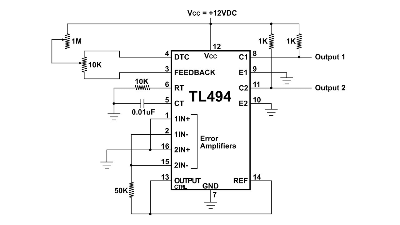
How to Use TL494?
 TL494 Pulse Width Modulation Control Circuit
To use the TL494, a versatile PWM controller, start by connecting its ground pin to the inverting inputs of the error amplifiers for stable signal reception, and link the non - inverting inputs directly to the 5V reference pin (Pin 14) to provide a consistent voltage for comparison. Next, configure the Dead - Time Control (Pin 4) and Feedback (Pin 3) pins to regulate switching intervals and ensure output stability. The oscillator frequency, which determines the PWM switching speed, is set by an external resistor (RT, Pin 6) and capacitor (CT, Pin 5) using the formula f=RT⋅CT1.1. Internally, the oscillator generates a sawtooth waveform; the PWM comparator then compares this waveform with the outputs from the error amplifiers. When the sawtooth waveform is higher than the error signal, the power switches are activated, and the duty cycle is adjusted to keep the output voltage (usually around 5V) stable. This setup, using basic components like resistors and capacitors, enables efficient power regulation in applications ranging from DC - DC converters to motor drives.
Examples of Circuits Using the TL494
TL494 Solar Charger
A solar charger circuit can be built using the TL494 to create a steady 5V power supply, perfect for charging devices. The circuit operates through both voltage and current control. It ensures that the output remains at a stable 5V, providing your devices with the correct voltage. It regulates the current to prevent it from becoming too high, protecting the circuit from potential damage. This type of charger is used for solar-powered applications, helping to save energy and protect your devices.
TL494 Inverter Circuit
An inverter changes DC power (like from a battery) into AC power (like what you use in your home). The TL494 can be used to make an efficient inverter circuit that provides stable power, even when the load (devices connected) changes. In this setup, the TL494 switches the power back and forth quickly, making the conversion from DC to AC smoother. This is useful in home inverters or emergency power systems.
TL494 DC to DC Converter
A DC to DC converter takes one voltage and turns it into another. For example, you can use the TL494 to change 12V DC (like from a car battery) to 5V DC, great for charging USB devices. This circuit has several components that contribute to its functionality. The feedback loop ensures that the output voltage remains steady, while the frequency control adjusts the switching speed to maximize efficiency. The circuit includes protection features that safeguard it by preventing excessive current flow and shutting down in case of overheating. Overall, this type of circuit is ideal for powering small electronic devices.
TL494 Variable Frequency Drive (VFD)
A Variable Frequency Drive (VFD) is used to control the speed of motors. With the TL494, you can build a VFD that adjusts the frequency of power sent to a motor, helping it run at different speeds. This is good for saving energy and extending the life of the motor. The TL494 uses PWM control to generate a special signal that regulates the amount of power sent to the motor. A feedback system continuously monitors the motor's performance and adjusts the power to ensure smooth operation. Variable Frequency Drives (VFDs) are employed in machines such as conveyor belts or fans.
TL494 LED Dimmer
The TL494 can also be used to dim LEDs for lighting systems where adjustable brightness is required. This circuit can be used in homes, cars, or displays. The dimming control adjusts the brightness of the LEDs by modifying the PWM signal. Smooth operation prevents the LEDs from flickering during the dimming process, providing a consistent and stable output. Built-in safety features protect the LEDs from overheating that helps extend their lifespan. Though simple in design, this type of circuit is highly effective for creating energy-efficient lighting systems.
TL494 Circuit Diagram
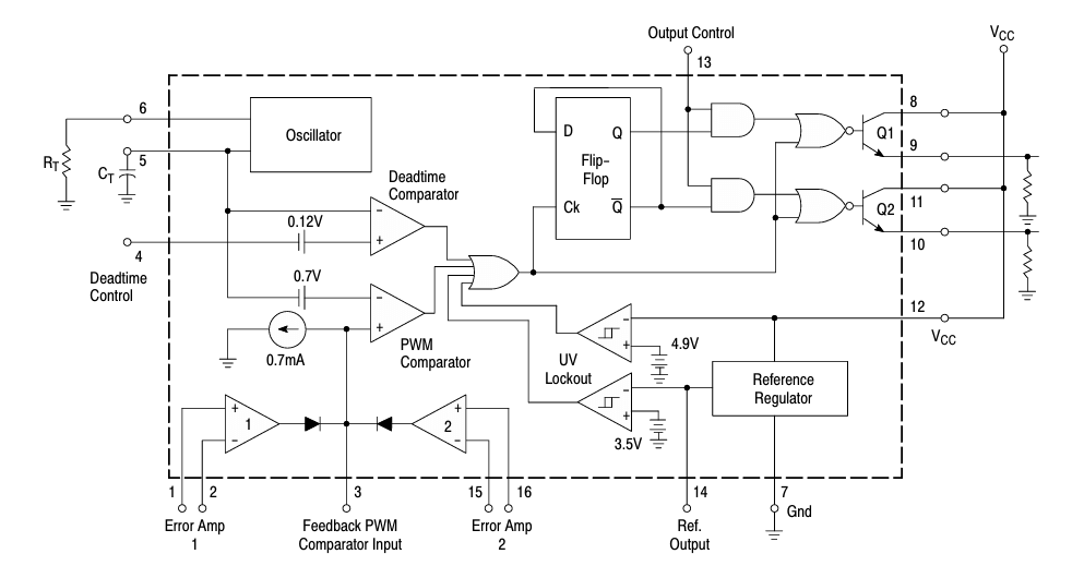 TL494 Circuit
The TL494 circuit diagram reveals its internal architecture and signal interactions. The oscillator, shaped by RT (pin 6) and CT (pin 5), generates a sawtooth waveform. A dead - time comparator (pin 4) adds a fixed offset (~0.12V) to limit the maximum duty cycle. Two error amplifiers (pins 1–2, 15–16) process feedback signals, which are OR - combined and fed to the PWM comparator to modulate the sawtooth - based duty cycle. A flip - flop, clocked by the oscillator, alternates outputs Q1/Q2 in push - pull mode (when pin 13 is high) or synchronizes them in single - ended mode (pin 13 low).
Timing Diagram
The TL494 timing diagram visualizes its internal signal interactions. The oscillator (shaped by RT/CT) generates a sawtooth waveform, forming the PWM time base. The dead - time control signal adds a fixed offset (~0.12V) to the sawtooth, ensuring a minimum off - time between pulses. The PWM comparator compares feedback (from error amplifiers) with the sawtooth, determining when output transistors switch on.
A flip - flop, clocked by the oscillator, produces complementary Q and Q signals. In push - pull mode (Output Control = High), Q and Q drive transistors Q1 and Q2 alternately, creating phase - opposite pulses with dead - time gaps. In single - ended mode (Output Control = Low), Q1 and Q2 switch synchronously, though dead - time still limits maximum duty cycle.
These timings coordinate error correction, frequency regulation, and power - switch protection, illustrating how the TL494’s internal blocks work together to deliver stable PWM control.
TL494 Manufacturer
The original developer of the TL494 is Texas Instruments (TI), which introduced the chip in the early 1980s. It established itself as an industry standard for power - supply control due to its high integration. As the market expanded, numerous semiconductor manufacturers rolled out compatible products: On the international front, Fairchild (now part of ON Semiconductor) offers the KA7500, a classic pin - compatible alternative with functions identical to those of the TL494. In the Chinese domestic market, local manufacturers such as Xinguang Youer also mass - produce the TL494 and its compatible chips, meeting the needs for cost - effectiveness and local supply. These compatible products are consistent with the original TI version in terms of pinout and electrical characteristics, allowing for direct replacement and supporting the continued widespread application of the TL494 in scenarios like switching power supplies and motor control.
TL494 Category-Current-Mode PWM Controller IC
A current-mode PWM controller IC is an integrated circuit designed for power management, regulating output voltage or current by adjusting pulse width. Unlike voltage-mode controllers, it employs a dual-loop feedback system: an inner current loop and an outer voltage loop, enabling precise current control and faster transient response. This architecture improves stability, reduces output ripple, and enhances short-circuit protection capabilities.
Key features include built-in error amplifiers, PWM comparators, oscillators, and dead-time controllers. Notable models like the TL494 and UC3842 integrate these functions, supporting topologies such as buck, boost, and full-bridge circuits. Current-mode control excels in high-power applications, offering better line and load regulation, making it ideal for switching power supplies, DC-DC converters, motor drives, and renewable energy systems. Its ability to quickly react to current spikes ensures safer operation and higher efficiency in demanding electronic designs.
TL494 Package
| Package |
Pins |
Size |
| PDIP (N) |
16 |
181 mm² 19.3 x 9.4 |
| SOIC (D) |
16 |
59 mm² 9.9 x 6 |
| SOP (NS) |
16 |
80 mm² 10.2 x 7.8 |
| TSSOP (PW) |
16 |
22 mm² 4.4 x 5 |

Alternative Solutions and Selection Recommendations
| Scenario |
Recommended IC |
Advantage Comparison |
| Low-power single-ended (<100W) |
UC3843 |
Pin-compatible with lower startup current (0.5mA vs. 5mA for TL494) |
| High-power push-pull (>300W) |
SG2525 |
Single-channel drive capability of 500mA, ideal for IGBT driving |
| Battery-powered devices |
TL3842 |
Wide voltage range (4.5–40V), suitable for automotive and PV applications |
| High-precision constant current |
UC2845 |
Built-in slope compensation, better suited for current-mode control |
After 30 years of market validation, the TL494 remains actively used in switching power supplies, motor control, new energy, and other fields, leveraging three key advantages: high integration, strong flexibility, and low cost. Its dual-error amplifier architecture is inherently suitable for constant voltage and constant current dual closed loops, while dead-time control and push-pull/single-ended switching simplify power stage design. The wide input voltage range of 7–40V further makes it a universal choice for both industrial and consumer electronics.
For beginners, starting with a single-ended buck circuit is recommended, while senior engineers can expand its boundaries through techniques like opto-coupler isolation and multi-chip synchronization. In the era of prevailing digital power supplies, the TL494's analog control characteristics have instead become a differentiated advantage of "strong anti-interference and fast response," especially suitable for cost-sensitive and reliability-critical scenarios. Mastering the TL494 is equivalent to holding a universal key to unlock the door of power supply design.
TL494 Frequently Asked Questions [FAQ]
1. What is the TL494 and its primary applications?
The TL494 is a dual-error-amplifier PWM controller IC designed for switch-mode power supply (SMPS) control. It supports push-pull, single-ended, and multi-phase topologies, making it ideal for ATX power supplies, battery chargers, industrial DC-DC converters, and solar inverters. Its dual-loop control (voltage + current) ensures precise regulation in applications up to 200W.
2. How do I set the switching frequency?
The frequency is set using external resistor RT (Pin 6) and capacitor CT (Pin 5). The formula is: f≈1.1/ RT⋅CT.
For example, RT=12kΩ and CT=0.01μF yield ~9kHz . Note that component tolerances and temperature may slightly affect the actual frequency.
3. What is the dead-time control range, and how does it work?
The dead time (time between switching transitions) is adjusted via Pin 4 (0–3.3V). It provides 5–100% control:
4. How to configure output modes (push-pull vs. single-ended)?
-
Push-pull mode: Connect Pin 13 to the 5V reference (Pin 14). Outputs 8 and 11 alternate with dead time, ideal for bridge topologies.
-
Single-ended mode: Connect Pin 13 to GND. Outputs 8 and 11 operate in parallel, suitable for single-switch converters .
5. What are the voltage and current limits for the TL494?
-
Supply voltage (Vcc): 7–40V (absolute maximum: 41V) .
-
Output current: Each transistor can source/sink 200mA continuous (250mA peak) .
-
Reference voltage: 5V ±5% (Pin 14), used for feedback and bias .
6. How to implement overcurrent protection (OCP)?
Use Error Amplifier 2 (Pins 15/16) to monitor current via a sensing resistor. Set the trip point by adjusting the voltage on Pin 15. If the sensed voltage (Pin 16) exceeds Pin 15, the IC reduces duty cycle or shuts down.
7. Can the TL494 be synchronized with other controllers?
Yes. Connect the oscillator’s RT pin (Pin 6) to the 5V reference and feed a synchronized sawtooth signal to CT (Pin 5). This allows multi-chip synchronization for parallel operation or phase-shifted designs .
8. What PCB layout guidelines should I follow?
-
Short traces: Keep power paths (Vcc, outputs) short and wide to minimize inductance.
-
Ground planes: Separate analog and power grounds to reduce noise coupling.
-
Bypass capacitors: Place a 10–100nF capacitor near Vcc (Pin 12) and the reference pin (Pin 14) .
-
Thermal pads: Ensure adequate heat dissipation for high-power applications.
9. What is the difference between commercial (TL494C) and industrial (TL494I) grades?
10. What are common troubleshooting issues?
-
Unstable output voltage: Check feedback loop compensation, reference voltage stability, and noise coupling.
-
Excessive switching noise: Optimize dead time, add snubber circuits, or reduce switching frequency.
-
No output: Verify Vcc, ground connections, and oscillator operation (check Pin 5 for sawtooth waveform).
11. Are there alternatives to the TL494?
For higher power or advanced features, consider:
-
UCC28500: Current-mode controller for PFC and LLC converters.
-
LM5036: High-voltage, multi-phase controller for server PSUs.
-
SG3525: Similar to TL494 but with a single error amplifier.
12. Where can I find datasheets and application notes?
Official TI datasheets and reference designs are available on TI.com . For practical circuits, refer to application notes like "Designing Switching Voltage Regulators with the TL494" .
For purchasing genuine TL494 ICs with technical support, contact WlS Electronic via SALES@WLSCHIP.COM or live chat.
WlS Electronic maintains a substantial inventory of TL494 Current-Mode PWM Controller ICs, high-performance solutions for precise power management and switch-mode power supply control in smart electronics. Sourced directly from leading manufacturers, all components are guaranteed genuine and brand-new, with comprehensive quality assurance protocols to ensure reliability in critical applications. For technical verification, detailed datasheets and application notes (e.g., dual-loop control designs, multi-phase synchronization) can be provided upon request.
Quick Quote & Support:
To request a quotation, fill in the quantity, your name, and email in the form on the right. Our sales team will respond within 12 hours. For urgent inquiries:
- Contact us via live chat support.
- Email us at: SALES@WLSCHIP.COM


