In the intricate world of digital electronics, where information is processed and transmitted as binary signals, the ability to store and synchronize data is paramount. Among the fundamental building blocks that enable this functionality, the D flip-flop stands out as a versatile and indispensable component. From simple registers to complex microprocessors, D flip-flops play a critical role in ensuring the reliable operation of digital systems. This article provides a comprehensive exploration of D flip-flops, covering their structure, working principles, types, applications, and practical considerations.
What is a D Flip-Flop?
A D flip-flop, short for "delay flip-flop" or "data flip-flop", is a key sequential logic component in digital electronics designed to store a single bit of binary data. It belongs to the family of flip-flops, which are edge-triggered memory devices, distinguishing them from level-triggered latches.
Unlike combinational logic circuits where output depends solely on current inputs, sequential logic circuits like D flip-flops incorporate memory, meaning their output depends on both present inputs and past states. This memory capability is essential for building complex digital systems such as microprocessors, registers, and counters.
D Flip-Flop Basic Structure and Symbol
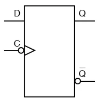 D Flip-Flop Symbol
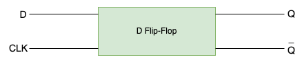 Block Diagram of D Flip Flop
- Data input (D): Carries the binary information to be stored
- Clock input (CLK or C): Provides the timing signal that controls data capture
- Output (Q): Delivers the stored binary value
- Complementary output (Q̅): Delivers the inverse of the stored value (always opposite to Q)
In circuit diagrams, the D flip-flop is represented by a rectangular symbol with the inputs and outputs labeled appropriately. The clock input typically includes a small triangle to indicate edge triggering, distinguishing it from level-sensitive latches.
A D flip-flop is created by modifying an SR flip-flop. The S input is connected to the D input, and the R input is connected to the inverted D input. As a result, a D flip-flop functions similarly to an SR flip-flop, but with complementary inputs, preventing any possibility of an invalid intermediate state. One major issue with the SR flip-flop is the race around condition, which is eliminated in the D flip-flop due to the inverted inputs. The circuit diagram of the D flip-flop is shown in the figure below:
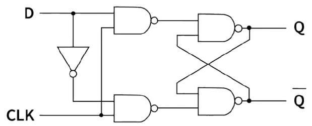 circuit diagram of the D flip-flop
Working of D Flip Flop
D flip flop consist of a single input D and two outputs (Q and Q'). The basic working of D Flip Flop is as follows:
- When the clock signal is low, the flip flop holds its current state and ignores the D input.
- When the clock signal is high, the flip flop samples and stores D input.
- The value that was previously fed into the D input is reflected at the flip flop's Q output.
- If D = 0 then Q will be 0.
- If D = 1 then Q will be 1.
- The Q' output of the flip flop is complemented by the Q output.
- If Q = 0 then Q' will be 1.
- If Q = 1 then Q' will be 0.
Characteristic Table of D Flip Flop
| CLK |
D |
Q (Next State) |
Q' |
| 0 (LOW) |
X |
Q (unchanged) |
Q' |
| ↑ (rising edge) |
0 |
0 |
1 |
| ↑ (rising edge) |
1 |
1 |
0 |
| 1 (HIGH, no edge) |
X |
Q (unchanged) |
Q' |
This table illustrates that a D flip-flop updates its output only on the rising edge of the clock signal that is, when the clock transitions from LOW to HIGH. At all other times, it maintains its previous output, ignoring any changes at the data input. This predictable, edge-sensitive behavior makes the D flip-flop valuable in digital systems where precise timing and sequence control are needed.
Flip-Flops Internal Circuitry
While the external behavior of a D flip-flop is straightforward, its internal structure involves clever arrangements of logic gates to achieve edge-triggered operation. The most common implementations include:
Gated D Latch with Pulse Detector
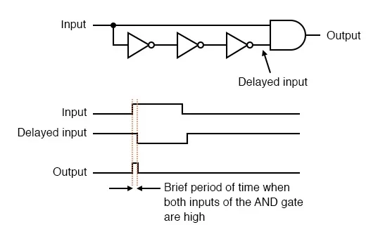 Pulse Detector
Master-Slave Configuration
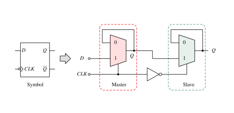 Master-Slave
SR Latch Modification
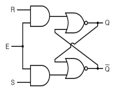 SR Latch
D Flip-Flops Applications
D flip-flops are fundamental building blocks in digital electronics, valued for their ability to store binary data and synchronize operations with a clock signal. Their simplicity and reliability make them indispensable in a wide range of applications, from basic storage to complex sequential circuits. Below are key application scenarios:
Data Storage and Registers
The primary function of a D flip-flop is to store a single bit of data (0 or 1) until the next clock edge. When multiple D flip-flops are connected in parallel, they form a register—a circuit that stores multiple bits of data simultaneously.
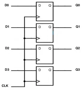 Parallel Registers
Parallel Registers: Used in microprocessors, memory units, and data buffers to hold temporary data during processing. For example, an 8-bit register (composed of 8 D flip-flops) can store a byte of data, which is critical for arithmetic operations in CPUs.
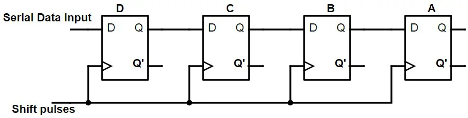 Shift Registers
Shift Registers: By connecting D flip-flops in series (where the output of one flip-flop feeds the input of the next), data can be shifted sequentially with each clock pulse. Shift registers are used in serial-to-parallel or parallel-to-serial data conversion (e.g., in UART communication) and for generating delay signals.
Synchronous Counters
D flip-flops are essential components in synchronous counters, which count clock pulses in a controlled sequence (e.g., binary, decimal). Unlike asynchronous counters, all flip-flops in a synchronous design are triggered by the same clock signal, ensuring precise timing.
Binary Counters: Each flip-flop represents a bit in the binary count. By feeding the inverted output (¬Q) of one flip-flop to the D input of the next, the counter increments by 1 with each clock pulse (e.g., 000 → 001 → 010...).
Up/Down Counters: Adding logic gates to control the D inputs allows the counter to count upward or downward based on a control signal, useful in applications like digital timers or position encoders.
Clock Synchronization
In digital systems with multiple subsystems, signals from different sources may have timing mismatches (skew). D flip-flops act as synchronizers to align these signals with the system clock, preventing metastability (an undefined state caused by timing violations).
Example: When a slow external sensor signal interacts with a high-speed microcontroller, a D flip-flop samples the sensor signal at each clock edge, ensuring the microcontroller receives stable, synchronized data.
Frequency Division
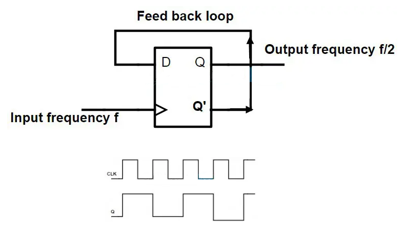 Frequency Division
Cascading such flip-flops creates higher frequency dividers (e.g., dividing by 4, 8, 16, etc.). These are used in clock generators for digital devices, where different subsystems require lower frequencies than the main clock (e.g., LCD displays, serial communication modules).
Memory Elements in Digital Systems
D flip-flops form the core of random-access memory (RAM) cells and read-only memory (ROM) address decoders. In RAM, each cell uses a D flip-flop to store a bit, with address lines controlling which cell is read or written. This enables fast, random access to data—critical for computer memory and embedded systems.
State Machines
Sequential logic circuits (e.g., finite state machines) rely on D flip-flops to store the current "state" of the system. The state determines how the circuit responds to inputs, making state machines essential for:
Control Units: Managing operations in microprocessors, where the sequence of instructions (fetch, decode, execute) is controlled by states stored in flip-flops.
Traffic Light Controllers: Cycling through states (red → yellow → green) based on clock pulses and sensor inputs.
Password Locks: Verifying input sequences by comparing stored states (correct digits) with user inputs.
Pulse Width Modulation (PWM)
In PWM circuits, which control devices like motors or LEDs, D flip-flops help generate stable pulse signals with adjustable duty cycles. By comparing a reference voltage with a ramp signal using a flip-flop, the output pulse width is modulated, regulating power delivery to the load.
Advantages of D Flip-Flops
Simplicity: With only one data input, it is easier to design and analyze than SR or JK flip-flops.
Predictable behavior: Eliminates the undefined states that plague SR flip-flops when both inputs are high.
Fast operation: Requires minimal logic gates, enabling high-speed performance with low propagation delay.
Design flexibility: Easily configurable for either rising or falling edge triggering.
Power efficiency: Simple structure consumes less power than more complex flip-flop types.
Scalability: Combines easily with other D flip-flops to create multi-bit storage structures.
Synchronous compatibility: Ideal for synchronous systems where all components operate from a common clock.
Limitations and Considerations
Despite their advantages, D flip-flops have limitations that designers must address:
Glitch sensitivity: Rapid changes in the D input near the clock edge can cause temporary output instability (glitches).
Timing constraints: Require specific setup and hold times—minimum periods before and after the clock edge when the D input must remain stable—to ensure reliable operation.
No inherent toggle function: Unlike T flip-flops, they cannot toggle states with each clock pulse without external feedback circuitry.
Metastability risk: If the D input changes precisely at the clock edge, the flip-flop may enter an unstable metastable state, taking unpredictable time to resolve to a valid logic level.
Limited functionality: Provides only basic storage, requiring additional logic for more complex operations.
Practical Implementation and ICs
D flip-flops are available as discrete integrated circuits (ICs) and are also fundamental building blocks in custom digital designs. Common IC implementations include:
- 74LS74 (TTL): Dual rising-edge triggered D flip-flops with preset and clear
- 74HC74 (CMOS): High-speed CMOS equivalent of the 74LS74
- CD4013 (CMOS): Dual D flip-flops with complementary outputs
- 74LS373/74HC373: Octal D latches with tri-state outputs (commonly used as address latches)
In modern digital design, D flip-flops are rarely implemented from discrete gates; instead, designers use hardware description languages (HDLs) like VHDL or Verilog to instantiate them, with synthesis tools converting the descriptions into optimized circuit layouts for ASICs or FPGAs.
The D flip-flop is arguably the most important memory element in digital electronics due to its simplicity, reliability, and versatility. Its ability to sample and hold data at precise clock edges makes it indispensable for synchronous digital systems. By eliminating the ambiguities of other flip-flop types while maintaining memory functionality, D flip-flops serve as the fundamental building blocks for constructing complex digital circuits ranging from simple registers to advanced microprocessors.
Understanding D flip-flops is essential for anyone working with digital systems, as they form the foundation of all sequential logic operations and data storage mechanisms in modern electronics.
WlS Electronic maintains a substantial inventory of D flip-flops ICs, high-performance solutions for digital signal storage and synchronization in smart electronics. Sourced directly from leading manufacturers, all components are guaranteed genuine and brand-new, with comprehensive quality assurance protocols in place. For technical verification, detailed datasheets and application notes can be provided upon request.
Quick Quote & Support:
To request a quotation, fill in the quantity, your name, and email in the form on the right. Our sales team will respond within 12 hours. For urgent inquiries:
Contact us via live chat support.
Email us at: SALES@WLSCHIP.COM
Trust WlS Electronic for reliable D flip-flops ICs that deliver precise signal handling for the most demanding applications—from consumer electronics to industrial IoT solutions.


