The ADI LT1012CN8#PB is a precision operational amplifier designed for applications demanding ultra-low offset voltage (25μV max), minimal bias current (±100pA max), and exceptional stability over temperature (0.6μV/°C drift). Part of the LT1012 series, it features internal compensation for unity-gain stability, simplifying circuit design. With low noise (0.5μV P-P from 0.1–10Hz) and wide supply range (±1.2V to ±20V), it suits both battery-powered and industrial systems. Ideal for high-impedance sensors, precision instrumentation, and medical devices, it directly replaces legacy OP-07 op-amps with 8x lower power and 20x reduced bias current. Available in an 8-pin PDIP package, it balances high performance with ease of use for critical applications requiring uncompromising accuracy.
ADI LT1012CN8#PB's Features
High Precision Performance
- Input Offset Voltage (VOS): Maximum 25μV (typical 8μV at 25°C), supports external nulling (±800μV adjustment range) to ensure low DC error.
- Bias Current (IB): Maximum ±100pA (typical ±25pA at 25°C), suitable for high-impedance signal sources (e.g., sensors, charge integrators).
- Offset Voltage Drift: Maximum 0.6μV/°C (typical 0.2μV/°C), excellent long-term stability (0.3μV/month).
Low Noise & High Stability
- Noise Performance: 0.5μV Peak-Peak noise over 0.1Hz to 10Hz, 17nV/√Hz noise density at 10Hz, and 14nV/√Hz at 1kHz, ideal for amplifying weak signals.
- Common-Mode Rejection Ratio (CMRR)/Power Supply Rejection Ratio (PSRR): Minimum 114dB for both, strong resistance to common-mode interference.
Low Power & Wide Supply Range
- Supply Current: Maximum 500μA (typical 370μA), supports ±1.2V to ±20V power supplies, suitable for battery-powered devices (e.g., two NiCd cells).
- Output Capability: Provides 5mA load current, voltage gain up to 1,000,000, and output swing of ±13V (RL=10kΩ, ±15V supply).
Wide Temperature Range & Reliability
- Operating Temperature: 0°C to 70°C (LT1012C model), storage temperature -65°C to 150°C, suitable for industrial applications.
- Internal Compensation: Unity gain stable, no external compensation capacitor required, simplifying circuit design.
Application Compatibility
- Direct replacement for OP-07, with 1/8th the power consumption and 1/20th the bias and offset currents.
- Suitable for high-precision scenarios such as precision instruments, charge integrators, thermocouple amplifiers, low-frequency filters, and optical measurements.
Electrical Parameters Summary
| Parameter |
Typical/Range |
Unit |
| Input Offset Voltage (VOS) |
25μV (max) |
μV |
| Bias Current (IB) |
±100pA (max) |
pA |
| Offset Voltage Drift |
0.6μV/°C (max) |
μV/°C |
| 0.1-10Hz Noise |
0.5μV Peak-Peak |
μV |
| Supply Current (IS) |
370μA (typ), 500μA (max) |
μA |
| CMRR/PSRR |
114dB min |
dB |
| Supply Voltage Range |
±1.2V to ±20V |
V |
Package & Pins
- Package: 8-pin PDIP (N8 package), pin definitions include inputs, output, power, null, and compensation terminals.
- Thermal Characteristics: θJA = 130°C/W, maximum junction temperature 100°C, stable operation in standard temperature environments.
ADI LT1012CN8#PB's Applications
1. Precision Measurement & Instrumentation
Sensor Signal Conditioning
High-Impedance Sensors: Suitable for amplifying signals from capacitive, piezoelectric, or resistive sensors (e.g., pressure transducers, strain gauges) due to its ultra-low bias current (±100pA maximum) and low input offset voltage (25μV maximum), minimizing signal distortion.
Thermocouple/RTD Amplification: Used in temperature measurement systems to amplify weak thermoelectric signals from thermocouples or resistance temperature detectors (RTDs), leveraging its low drift (0.6μV/°C max) and high CMRR (114dB min) to reject common-mode noise.
Multimeters & Calibration Equipment: Ensures high-resolution measurements in test instruments by maintaining minimal DC errors and stable gain over temperature.
Analog-to-Digital (A/D) Pre-Amplification
Boosts low-level signals before conversion to digital, improving the effective resolution of A/D converters through low noise (0.5μV P-P in 0.1–10Hz) and precise offset control.
2. Low-Power & Battery-Powered Systems
Portable Electronics
Handheld Devices: Powers battery-operated analyzers, dataloggers, or medical monitors with low supply current (370μA typ), supporting wide input voltages (±1.2V to ±20V) for flexibility with battery chemistries (e.g., NiCd, Li-ion).
Wireless Sensor Nodes: Enables long battery life in IoT or remote monitoring systems by balancing low power consumption with high-precision signal processing.
3. High-Accuracy Analog Signal Processing
Filtering & Signal Conditioning
Low-Frequency Filters: Designs precision active filters (e.g., Butterworth, Chebyshev) for audio, biomedical, or industrial signals, benefiting from unity-gain stability and low noise at both low (17nV/√Hz at 10Hz) and high (14nV/√Hz at 1kHz) frequencies.
Integrators & Differentiators
Precision Integrators: Used in analog-to-digital conversion (e.g., dual-slope ADCs) where drift and offset stability are essential.
Charge Integrators: Processes charge signals from photomultipliers or particle detectors with minimal bias current error, critical for applications like spectroscopy or laser measurement.
Logarithmic/Exponential Amplifiers
Implements nonlinear signal processing for applications like optical power measurement or dynamic range compression, utilizing low offset voltage to maintain accuracy across input ranges.
4. Industrial & Scientific Equipment
Process Control & Automation
Amplifies signals from industrial sensors (e.g., flow meters, level sensors) in harsh environments, with a wide storage temperature range (-65°C to 150°C) and robust PSRR (114dB min) to reject power supply noise.
Optical Systems
Photodiode Amplification: Converts low-level photocurrents to voltage in optical receivers, spectrometers, or laser rangefinders, leveraging ultra-low bias current and high input impedance to minimize loading effects.
Imaging Subsystems: Enhances signal quality in CCD/CMOS sensor readout circuits, reducing noise and improving linearity.
5. Medical & Biomedical Applications
Biopotential Amplification
Amplifies weak bioelectrical signals (e.g., ECG, EEG, EMG) with high CMRR to reject mains interference and low noise to avoid masking small signals (e.g., μV-level neural signals).
Medical Instruments
Used in blood pressure monitors, glucose meters, or portable diagnostic devices, combining low power with high precision for reliable patient data acquisition.
6. Replacement for Legacy Precision Op-Amps
Drop-In Replacement for OP-07
Offers 8x lower power consumption and 20x lower bias/offset currents than the OP-07, making it an optimal upgrade in existing designs without significant circuit redesign, while improving stability and noise performance.
Typical circuit examples
- Basic Inverting/Non-Inverting Amplifier: Uses external null pins (Pins 1 and 5) to further reduce offset voltage for critical DC accuracy.
- Charge Integrator: Connects a feedback capacitor to the inverting input, leveraging low bias current to minimize charge leakage errors over time.
- Differential Amplifier for Thermocouples: Employs high CMRR to reject noise from long sensor cables, with gain set by external resistors for precise temperature scaling.
ADI LT1012CN8#PB's Attributes
| Package |
Tube |
Product Status |
Active |
| Amplifier Type |
General Purpose |
Number of Circuits |
1 |
| Slew Rate |
0.2V/µs |
Current - Input Bias |
30 pA |
| Voltage - Input Offset |
10 µV |
Current - Supply |
380µA |
| Voltage - Supply Span (Min) |
2.4 V |
Voltage - Supply Span (Max) |
40 V |
| Operating Temperature |
0°C ~ 70°C |
Mounting Type |
Through Hole |
| Package / Case |
8-DIP (0.300", 7.62mm) |
Supplier Device Package |
8-PDIP |
| Base Product Number |
LT1012 |
|
|

ADI LT1012CN8#PB's Symbol, Footprint and 3D Model
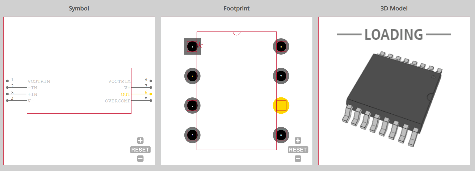
The ADI LT1012CN8#PB utilizes an 8-pin PDIP (Plastic Dual In-line Package, N8 package) with the following pinout configuration. Pin numbering follows the standard DIP layout (viewed from the top with the notch facing left):
Pinout Diagram & Function Description
| Pin # |
Label |
Function |
| 1 |
OFFSET NULL 1 |
External offset nulling terminal (connect to a potentiometer with pin 5) to adjust input offset voltage. |
| 2 |
IN- (Inverting Input) |
Inverting input terminal. Connect the negative (or reference) side of the signal source for inverting amplification. |
| 3 |
IN+ (Non-Inverting Input) |
Non-inverting input terminal. Connect the positive side of the signal source for non-inverting amplification or voltage-follower configuration. |
| 4 |
V- (Negative Supply) |
Negative power supply input. Supports ±1.2V to ±20V (typically connected to -15V in standard systems). |
| 5 |
OFFSET NULL 2 |
External offset nulling terminal (paired with pin 1). See offset adjustment notes below. |
| 6 |
OUT (Output) |
Output terminal. Provides the amplified signal to the load (max 5mA output current, ±13V swing with ±15V supply and 10kΩ load). |
| 7 |
V+ (Positive Supply) |
Positive power supply input. Supports ±1.2V to ±20V (typically connected to +15V in standard systems). |
| 8 |
NC (No Connection) |
No internal connection (floating). Leave unconnected in most applications. |
Key Notes on Pin Functions
Offset Nulling (Pins 1 and 5)
To further reduce input offset voltage (VOS), connect a 10kΩ potentiometer between pins 1 and 5, with the wiper terminal connected to the negative supply (V-). Adjust the potentiometer to minimize output offset under zero-input conditions.
Factory calibration may make external nulling unnecessary for many applications, but it offers additional precision when required.
Power Supply Pins (Pins 4 and 7)
Decouple V+ and V- with 100nF ceramic capacitors placed close to the package to suppress high-frequency noise, especially in noisy environments.
The wide supply range (±1.2V to ±20V) supports both low-voltage battery systems (e.g., ±1.5V from two NiCd cells) and standard ±15V industrial setups.
Input Pins (Pins 2 and 3)
Low Bias Current: The ultra-low bias current (±100pA max) ensures compatibility with high-impedance sensors (e.g., capacitive, piezoelectric) without significant loading error.
Ensure input signals remain within the common-mode voltage range (typically within 2V of the supply rails for optimal performance).
Output Pin (Pin 6)
The output is internally compensated for unity gain stability, eliminating the need for external compensation capacitors (simplifies circuit design compared to older op-amps).
Maximum output current is 5mA, suitable for driving moderate loads (e.g., 10kΩ resistors) or feeding into high-impedance stages.
ADI LT1012CN8#PB's Category-operational amplifier
An operational amplifier (op-amp) is a fundamental analog integrated circuit designed to amplify voltage signals with high precision and versatility. It features two input terminals—an inverting input (marked “−”) and a non-inverting input (marked “+”)—and a single output. Key characteristics include extremely high open-loop voltage gain (often exceeding 100,000), high input impedance (minimizing current draw from the input source), low output impedance (enabling drive capability for loads), and the ability to operate with both positive and negative power supplies. Op-amps excel in various applications, from basic signal amplification (inverting/non-inverting configurations) to complex tasks like filtering, integration, differentiation, and voltage comparison. Critical performance parameters include input offset voltage (VOS, the voltage needed to null the output with zero input), bias current (IB, the current drawn by the input terminals), noise density, common-mode rejection ratio (CMRR) (rejection of unwanted common signals), and power supply rejection ratio (PSRR). These parameters determine an op-amp’s suitability for precision tasks, such as sensor signal conditioning, medical instrumentation, or high-accuracy measurements.
Modern op-amps like the ADI LT1012CN8#PB exemplify advanced precision design. It offers ultra-low VOS (25μV max), negligible bias current (±100pA max), and minimal drift (0.6μV/°C max), making it ideal for amplifying weak signals from high-impedance sensors like piezoelectric transducers or thermocouples. With low noise (0.5μV P-P in 0.1–10Hz) and internal unity-gain compensation, it simplifies circuit design while ensuring stability. Its wide supply range (±1.2V to ±20V) and low power consumption (370μA typical) make it suitable for both battery-powered devices and industrial systems. As a direct replacement for legacy models like the OP-07 with 8x lower power and 20x lower bias current, the LT1012CN8#PB sets a standard for precision, reliability, and efficiency in applications demanding uncompromising signal integrity.
LT1012CN8#PB's Manufacturer-ADI
Analog Devices (ADI) has established itself as a pioneering force in the operational amplifier (op-amp) domain, driving innovation and setting industry standards for over five decades. Since its founding in 1965 by Ray Stata and Matthew Lorber, the company has been at the forefront of developing high-performance op-amps, targeting emerging markets with groundbreaking solutions. In 1974, ADI introduced the AD520, the first monolithic instrumentation amplifier, revolutionizing precision measurement systems. Four years later, the AD571 marked a milestone as the industry’s first monolithic analog-to-digital converter, followed by the AD574 in 1980, which became the go-to 12-bit A/D converter with microprocessor compatibility, solidifying ADI’s role in digital integration. ADI’s op-amp portfolio is renowned for its diversity and excellence, catering to markets like automotive, industrial, and healthcare. The company offers specialized solutions such as JFET-input op-amps for high-speed applications requiring ultra-low input bias current, and low-power variants that extend battery life while minimizing thermal drift. Its low-noise op-amps, with noise levels as low as 2 nV/√Hz (e.g., the ADA4004-4), excel in precision-critical environments, while high-voltage models like the AD8675 deliver robust performance in industrial systems. A key innovation is the zero-drift technology, which continuously corrects DC errors over time and temperature, ensuring stability in challenging conditions. The 2016 acquisition of Linear Technology further strengthened ADI’s op-amp dominance, combining two industry leaders with complementary strengths in analog ICs. While the merger addressed concerns about competition, it also unified decades of expertise, enabling advancements in miniaturization (e.g., 3mm x 3mm packages) and power efficiency (40% lower consumption in devices like the AD8677). Today, ADI’s op-amps are celebrated for their balance of performance, reliability, and integration, empowering applications from automated test equipment to portable medical devices. With a legacy of technical breakthroughs and a commitment to addressing evolving market needs, ADI remains a driving force in shaping the future of operational amplifier technology.
LT1013CN8#PBF vs LT1012CN8#PBF
| Picture |
 |
 |
| Part Number |
LT1013CN8#PBF +BOM |
LT1012CN8#PBF +BOM |
| Manufacturer |
Analog Devices, Inc |
Analog Devices, Inc |
| Package |
DIP-8 |
PDIP-8 |
| Description |
General Purpose Amplifier 2 Circuit 8-PDIP |
General Purpose Amplifier 1 Circuit 8-PDIP |
| Stock |
1549 |
2385 |
| Number of Channels |
2 Channel |
1 |
| Current - Input Bias |
12 nA |
30 pA |
| Input Bias Current |
200 pA |
150nA (max) |
| Product Type |
Precision Amplifiers |
Precision Operational Amplifier |
| RoHS |
True |
- |
| GBP - Gain Bandwidth |
800 kHz |
1.5MHz |
| SR - Slew Rate |
400 mV/μs |
0.5V/μs |
| Vos - Input Offset |
60 μV |
100µV (max) |
| Max Supply Voltage |
44 V |
40 V |
| Supply Voltage - Min |
4 V |
2.4 V |
| Current @ Pmpp |
350 uA |
380µA |
| Load Current |
25 mA |
- |
| CMRR |
117 dB |
- |
| Input Voltage Noise |
22 nV/√Hz |
- |
| Mounting Style |
Through Hole |
Through Hole |
| Auto Shutdown |
No Shutdown |
- |
| Temp Range (Min) |
0°C |
-40°C |
| Temp Range (Max) |
+70°C |
+85°C |
| Series |
LT1013 |
LT1012 |
| Gain V/V |
7 V/μV |
- |
| Input Noise Current |
0.07 pA/rtHz |
- |
| PSRR |
117 dB |
- |
| Factory Pack Qty |
50 |
- |
| Unit Weight |
0.560009 oz |
- |
| Product Name |
- |
LT1012CN8#PBF |
| Supply Voltage Range |
+/-5V to +/-18V (implied) |
+/-5V to +/-18V |
| Package/Case |
8-DIP (0.300", 7.62mm) |
PDIP-8 |
| Product Status |
Active |
Active |
| Amplifier Type |
General Purpose |
General Purpose |
| Voltage - Input Offset |
- |
10 µV |
| Voltage - Supply Span |
4V to 44V |
2.4V to 40V |
| Operating Temperature |
0°C ~ 70°C |
-40°C to +85°C |
| Supplier Device Package |
8-PDIP |
8-PDIP |
| Base Product Number |
LT1013 |
LT1012 |
WlS Electronic holds a large inventory of Analog Devices LT1012CN8#PBF. We assure you that these are genuine and brand-new components, directly sourced from Analog Devices. If needed, we can provide quality test reports for the LT1012CN8#PBF. To obtain a quotation, simply fill in the desired quantity, your contact name, and your email address in the quick quotation form on the right. Our sales representatives will get in touch with you within 12 hours. You can contact us online at any time, or send an email to: SALES@WLSCHIP.COM.


