The TDA2030 stands as a foundational audio power amplifier IC renowned for its enduring popularity in low-to-mid power audio systems. Developed by STMicroelectronics, this compact yet robust chip balances simplicity, performance, and cost-effectiveness—making it a staple for engineers, hobbyists, and consumer electronics alike. In this guide, we’ll dissect its core features (class-AB operation, integrated protection, and flexible gain), map its diverse applications (from home stereos to car audio), decode critical specs from its datasheet (power limits, distortion, and thermal behavior), and demystify its pinouts for seamless circuit design.
TDA2030 Audio Amplifier Overview
The TDA2030 is a monolithic integrated low-frequency class AB amplifier launched by STMicroelectronics. It adopts the Pentawatt® package and is specifically designed for low-frequency signal amplification scenarios such as audio amplification.
Its core performance is as follows: With a 14V power supply, 4Ω load, and 0.5% distortion rate, the typical output power reaches 14W; with ±14V or 28V power supply, it guarantees an output power of 12W under a 4Ω load and 8W under an 8Ω load (in compliance with the DIN45500 standard).
The core advantages of this device lie in its high output current capability, extremely low harmonic and crossover distortion. Meanwhile, it integrates a patented short-circuit protection system (which ensures output transistors operate in the safe region by automatically limiting power consumption) and a conventional thermal shutdown function, greatly enhancing operational stability and reliability.
TDA2030 Audio Amplifier Pinouts
| Pin Number |
Function Definition |
Remarks |
| Pin 1 |
Non-inverting Input |
Receives positive input signals |
| Pin 2 |
Inverting Input |
Receives negative input signals |
| Pin 3 |
Negative Power Supply (-Vs) |
The package tab is connected to this pin for heat dissipation |
| Pin 4 |
Positive Power Supply (+Vs) |
Connects to positive power supply voltage |
| Pin 5 |
Output |
Outputs the amplified signal |
TDA2030 Audio Amplifier Specifications
| Parameter |
Value |
| Package/Case |
Pentawatt-5 (Vertical, Bent and Staggered Leads) |
| Operating Temperature |
-40°C ~ 150°C TJ |
| JESD-609 Code |
E3 |
| Moisture Sensitivity Level (MSL) |
1 (Unlimited) |
| ECCN Code |
EAR99 |
| Terminal Finish |
Matte Tin (Sn) |
| Base Part Number |
TDA2030 |
| Qualification Status |
Not Qualified |
| Operating Supply Voltage |
28V |
| Nominal Current |
80mA |
| Output Current |
3.5A |
| Output Power |
14W |
| Input Offset Voltage (VOS) |
20mV |
| Power Supply Rejection Ratio (PSRR) |
50dB |
| Maximum Dual Supply Voltage |
18V |
| Minimum Dual Supply Voltage |
6V |
| Input Bias Current |
2µA |
| Harmonic Distortion |
10% |
| Load Impedance |
4Ω |
| Reach SVHC |
No SVHC |
| Pins |
- |
TDA2030 Audio Amplifier Absolute Maximum Ratings
The following table lists the absolute maximum ratings of the TDA2030. Exceeding these ranges may cause damage to the device:
| Parameter |
Symbol |
Value |
Unit |
| Supply Voltage |
Vs |
±18V (or 36V for single power supply) |
V |
| Input Voltage |
Vi |
Equal to supply voltage Vs |
- |
| Differential Input Voltage |
Vi |
±15V |
V |
| Peak Output Current (internally limited) |
Io |
3.5A |
A |
| Total Power Dissipation (Tc=90℃) |
Ptot |
20W |
W |
| Storage and Junction Temperature |
Tstg, Tj |
-40~150℃ |
℃ |
TDA2030 Audio Amplifier Electrical Parameters
Under the conditions of Vs=±14V and Tamb=25℃ (unless otherwise specified), the key electrical parameters of the TDA2030 are as follows :
| Parameter |
Symbol |
Test Conditions |
Typical Value |
Range |
Unit |
| Supply Voltage Range |
Vs |
- |
- |
±6~±18V (12~36V for single power supply) |
V |
| Quiescent Leakage Current |
Id |
- |
40mA |
40~60mA |
mA |
| Input Bias Current |
Ib |
Vs=±18V (36V for single power supply) |
0.2μA |
0.2~2μA |
μA |
| Input Offset Voltage |
Vos |
- |
±2mV |
±2~±20mV |
mV |
| Output Power (0.5% distortion) |
Po |
f=40~15kHz, Gv=30dB, RL=4Ω/8Ω |
14W/9W |
Minimum 12W/8W |
W |
| Frequency Response (-3dB) |
B |
Po=12W, RL=4Ω, Gv=30dB |
- |
10Hz~140kHz |
Hz |
| Input Resistance (Pin 1) |
Ri |
- |
5MΩ |
Minimum 0.5MΩ |
MΩ |
| Power Supply Rejection Ratio |
SVR |
Gv=30dB, RL=4Ω, 100Hz ripple |
50dB |
Minimum 40dB |
dB |
TDA2030 Audio Amplifier Features
The TDA2030 is a high-performance audio amplifier with the following key features:
- Wide Power Supply Compatibility: Supports a wide supply voltage range, up to 36 V, and is adaptable to both single power supply and split (dual) power supply configurations.
- High Output Power: Typically delivers 14 W output power at 14 V with a 4 Ω load (at 0.5% distortion). Under ±14 V or 28 V supply, it guarantees 12 W output on a 4 Ω load and 8 W on an 8 Ω load (compliant with DIN45500 standards).
- Low Distortion Performance: Features very low harmonic distortion and crossover distortion, ensuring high-fidelity audio output. For example, distortion (d) is typically 0.2% (max 0.5%) when output power ranges from 0.1 W to 12 W (4 Ω load) at 40–15,000 Hz.
- High Output Current: Provides high output current capability, suitable for driving various audio loads.
- Integrated Protection Mechanisms:
- Patented Short-Circuit Protection: Incorporates an original short-circuit protection system that automatically limits power dissipation, keeping output transistors within their safe operating range to prevent damage during accidental output-to-ground short circuits.
- Thermal Shutdown: Includes a conventional thermal shutdown system. The junction temperature (Tj) is restricted to a maximum of 150°C, and the system activates when Tj reaches 145°C, reducing power dissipation to avoid overheating damage.
- Versatile Packaging: Available in the Pentawatt® horizontal package (order code: TDA2030H), which facilitates heat dissipation and easy integration into circuits.
- Stable Electrical Characteristics: Offers stable performance with features like a wide frequency response (10 Hz to 140 kHz at -3 dB), high voltage gain (90 dB open-loop, 30 dB closed-loop at 1 kHz), and low noise (typical input noise voltage of 3 μV in 22 Hz–22 kHz bandwidth).
TDA2030 Functions
As a monolithic integrated low-frequency class-AB audio amplifier, the functions of the TDA2030 focus on efficient signal amplification, stable operation, and flexible adaptation. Its core functions are as follows:
1. Basic Audio Amplification Function
- Low-frequency signal power amplification: Designed for low-frequency audio signals in the 10Hz-140kHz range, it can amplify weak input signals to medium-power output, meeting the driving requirements of speakers.
- High current driving capability: The peak output current is internally limited to 3.5A, which can directly drive 4Ω or 8Ω speakers, adapting to common audio loads.
2. Low Distortion and High-Fidelity Signal Processing
- Low distortion characteristics: Through optimized circuit design, harmonic distortion and crossover distortion are significantly reduced. In the output power range of 0.1-12W (4Ω load) and frequency range of 40-15000Hz, the distortion rate (d) has a typical value of 0.2% and a maximum value of 0.5%; under 8Ω load, the typical value is as low as 0.1%, ensuring pure reproduction of audio signals.
- Stable gain control: The typical value of open-loop voltage gain is 90dB, and the closed-loop voltage gain (at 1kHz) is stable at 30dB (ranging from 29.5-30.5dB), ensuring that input signals are amplified in a fixed proportion and avoiding the impact of gain fluctuations on sound quality.
- Low noise performance: The input noise voltage is low (typical value of 3μV and maximum value of 10μV within the 22Hz-22kHz bandwidth), and the typical value of input noise current is 200pA, reducing interference to weak input signals.
3. Wide Power Supply Adaptation and Flexible Power Supply
- Wide voltage range support: Compatible with dual power supplies (±6V to ±18V) and single power supplies (12V to 36V), with a maximum withstand voltage of 36V, adapting to different power supply scenarios such as vehicle-mounted and household use.
- Power supply rejection capability: The typical value of Power Supply Rejection Ratio (SVR) is 50dB (under 100Hz ripple), which can effectively suppress noise caused by power supply fluctuations and ensure stable output signals.
4. Built-in Protection Mechanisms (Core Reliability Guarantee)
- Patented short-circuit protection: When the output is accidentally short-circuited to the ground, it automatically limits the power dissipation of the output transistors (instead of simple current limiting) to ensure they work within the Safe Operating Area (SOA), avoiding damage due to overcurrent or overpower. The protection logic is dynamically adjusted with the voltage drop (VCE) of the output tube to balance power and safety.
- Thermal shutdown protection: Integrates a thermal limiting circuit. When the junction temperature (Tj) rises to 145°C, protection is triggered, and power dissipation is automatically reduced to limit the junction temperature to no more than 150°C, which can withstand continuous overloads or high-temperature environments and avoid device damage due to overheating.
5. Frequency Response and Stability Guarantee
- Wide frequency response: The -3dB bandwidth is 10Hz-140kHz (at 12W output and 4Ω load), covering the full range of audible audio signals for the human ear, ensuring effective amplification of both high and low-frequency signals.
- High input impedance: The typical value of input resistance at pin 1 (non-inverting input) is 5MΩ (minimum 0.5MΩ), reducing the load on the front-end signal source and adapting to various signal input devices.
TDA2030 Audio Amplifier Applications
As a monolithic integrated low-frequency class-AB audio amplifier, the functions of the TDA2030 focus on efficient signal amplification, stable operation, and flexible adaptation. Its core functions are as follows:
1. Basic Audio Amplification Function
- Low-frequency signal power amplification: Designed for low-frequency audio signals in the 10Hz-140kHz range, it can amplify weak input signals to medium-power output, meeting the driving requirements of speakers.
- High current driving capability: The peak output current is internally limited to 3.5A, which can directly drive 4Ω or 8Ω speakers, adapting to common audio loads.
2. Low Distortion and High-Fidelity Signal Processing
- Low distortion characteristics: Through optimized circuit design, harmonic distortion and crossover distortion are significantly reduced. In the output power range of 0.1-12W (4Ω load) and frequency range of 40-15000Hz, the distortion rate (d) has a typical value of 0.2% and a maximum value of 0.5%; under 8Ω load, the typical value is as low as 0.1%, ensuring pure reproduction of audio signals.
- Stable gain control: The typical value of open-loop voltage gain is 90dB, and the closed-loop voltage gain (at 1kHz) is stable at 30dB (ranging from 29.5-30.5dB), ensuring that input signals are amplified in a fixed proportion and avoiding the impact of gain fluctuations on sound quality.
- Low noise performance: The input noise voltage is low (typical value of 3μV and maximum value of 10μV within the 22Hz-22kHz bandwidth), and the typical value of input noise current is 200pA, reducing interference to weak input signals.
3. Wide Power Supply Adaptation and Flexible Power Supply
- Wide voltage range support: Compatible with dual power supplies (±6V to ±18V) and single power supplies (12V to 36V), with a maximum withstand voltage of 36V, adapting to different power supply scenarios such as vehicle-mounted and household use.
- Power supply rejection capability: The typical value of Power Supply Rejection Ratio (SVR) is 50dB (under 100Hz ripple), which can effectively suppress noise caused by power supply fluctuations and ensure stable output signals.
4. Built-in Protection Mechanisms (Core Reliability Guarantee)
- Patented short-circuit protection: When the output is accidentally short-circuited to the ground, it automatically limits the power dissipation of the output transistors (instead of simple current limiting) to ensure they work within the Safe Operating Area (SOA), avoiding damage due to overcurrent or overpower. The protection logic is dynamically adjusted with the voltage drop (VCE) of the output tube to balance power and safety.
- Thermal shutdown protection: Integrates a thermal limiting circuit. When the junction temperature (Tj) rises to 145°C, protection is triggered, and power dissipation is automatically reduced to limit the junction temperature to no more than 150°C, which can withstand continuous overloads or high-temperature environments and avoid device damage due to overheating.
5. Frequency Response and Stability Guarantee
- Wide frequency response: The -3dB bandwidth is 10Hz-140kHz (at 12W output and 4Ω load), covering the full range of audible audio signals for the human ear, ensuring effective amplification of both high and low-frequency signals.
- High input impedance: The typical value of input resistance at pin 1 (non-inverting input) is 5MΩ (minimum 0.5MΩ), reducing the load on the front-end signal source and adapting to various signal input devices.
Typical application circuit
1. General Working Principle
Both circuits are dual-power (±Vs) class-AB audio amplifier configurations for the TDA2030. They leverage negative feedback to stabilize gain, reduce distortion, and integrate protection diodes to safeguard against voltage spikes from inductive loads (e.g., speakers).
2. TDA2030 Application Circuit 1
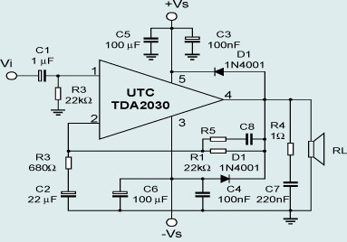 TDA2030 Application Circuit 1
| Component |
Value |
Role |
| Input Stage |
C1 = 1μF |
Blocks DC, couples audio signal to the non-inverting input (Pin 1). |
| |
R3 = 22kΩ |
Provides DC bias to Pin 1, stabilizing input voltage. |
| Feedback Network |
R1 = 22kΩ, R2 = 680Ω |
Forms voltage negative feedback. Closed-loop gain: G≈1+R2R1≈34 (≈31.6 dB). |
| |
C2 = 22μF |
Phase compensation capacitor, prevents high-frequency oscillation. |
| Output & Protection |
R4 = 1Ω |
Current-sensing resistor (supports overcurrent protection/stability). |
| |
D1 (2 pcs) |
Clamps output voltage within ±Vs, protecting the chip from inductive spikes. |
| Power Supply |
C3/C4 = 100nF |
High-frequency decoupling (filters power supply noise). |
| |
C5/C6 = 100μF |
Low-frequency decoupling (stabilizes power voltage). |
| |
C7 = 220nF |
Output high-frequency compensation (improves sound clarity). |
Features:
- High Gain: ~34x gain suits small input signals (e.g., weak audio sources like microphones).
- High Input Impedance: 22kΩ bias resistor minimizes loading on the front-end signal source.
- Standard Power Filtering: 100μF capacitors balance cost and noise reduction for general audio systems.
3.TDA2030 Application Circuit 2
Key Components & Functions:
|
Component
|
Value
|
Role
|
|
Input Stage
|
C1 = 1μF
|
Same as Circuit 1 (DC blocking, signal coupling).
|
|
|
R3 = 2.2kΩ
|
Lower bias resistor → reduces input impedance (suits low-source-impedance applications).
|
|
Feedback Network
|
R1 = 13kΩ, R3 = 680Ω
|
Closed-loop gain: G≈1+R3R1≈20 (≈26.1 dB). Lower gain reduces risk of input overload.
|
|
|
C2 = 22μF
|
Phase compensation (same as Circuit 1).
|
|
Output & Protection
|
R4 = 1Ω
|
Same as Circuit 1 (current sensing/protection).
|
|
|
D1 (2 pcs)
|
Same as Circuit 1 (spike protection).
|
|
Power Supply
|
C3 = 100nF
|
High-frequency decoupling (same as Circuit 1).
|
|
|
C5 = 220μF
|
Larger low-frequency capacitor → better ripple filtering (suits noisy power sources like car batteries).
|
|
|
C6 = 100μF
|
Low-frequency decoupling (same as Circuit 1).
|
|
|
C7 = 220nF
|
Output high-frequency compensation (same as Circuit 1).
|
TDA2030 Application Circuit 2
Features:
- Lower Gain: ~20x gain avoids clipping with large input signals (e.g., professional audio preamps).
- Lower Input Impedance: 2.2kΩ bias resistor suits low-impedance sources (e.g., digital audio players).
- Enhanced Power Filtering: 220μF capacitor improves stability in harsh power environments (e.g., vehicle audio).
TDA2030 test circuit
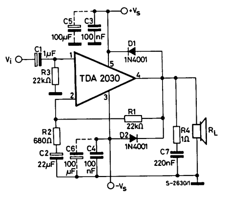
The TDA2030 test circuit operates with a dual - power (±Vs) supply and centers on a class - AB audio power amplifier chip. On the input side, a C1 (1μF) DC - blocking capacitor couples the audio signal to the non - inverting input, while R3 (22kΩ) provides DC bias to stabilize the operating point. The feedback network consists of R1 (22kΩ) as the negative feedback resistor, R2 (680Ω), and C2 (22μF) as the phase compensation capacitor, achieving a closed - loop gain of approximately 34 times to suppress self - oscillation.
On the power supply side, a combination of “100nF high - frequency capacitors + 100μF low - frequency capacitors” (C3/C5, C4/C6) performs filtering to eliminate ripple noise. D1/D2 (1N4001) clamping diodes protect the chip from damage caused by inductive spikes from the speaker. On the output side, R4 (1Ω) and C7 (220nF) form a Zobel network to compensate for the speaker’s high - frequency inductive impedance and prevent oscillation.
This circuit is used to verify the TDA2030’s power output, distortion, and stability, suitable for scenarios like home audio and car audio. Through modular design, it covers the full - process testing requirements of “signal amplification → power supply filtering → load protection”.
TDA2030 Alternatives
When seeking alternatives to the TDA2030, a range of audio amplifier ICs with similar low-frequency class AB operation, power output capabilities, and protection features can be considered. These alternatives are suitable for applications such as home audio systems, multimedia speakers, and small-scale public address setups, with varying degrees of compatibility in terms of power, package, and functionality:
A high-performance audio power amplifier, the LM1875 is a robust alternative to the TDA2030, offering slightly higher power and superior thermal stability.
- Output Power: 20W continuous output with low distortion, suitable for applications requiring marginally higher wattage than the TDA2030 (14W typical).
- Features: Overload protection, a wide supply voltage range (±16V to ±60V), and excellent linearity, ensuring low harmonic distortion.
- Package: 5-pin TO-220, compatible with heat sinks designed for the TDA2030, minimizing layout adjustments.
A dual-channel class AB amplifier, ideal for stereo applications where the TDA2030’s single-channel design may be limiting.
- Output Power: 6W per channel in stereo mode (4Ω load) or 18W in bridge mode, matching the TDA2030’s bridge configuration power (18W).
- Features: Integrated short-circuit and thermal protection, low distortion (typical 0.1%), and a compact SIP15 package.
- Compatibility: Requires minor PCB adjustments due to its 15-pin package but offers similar voltage range (10–18V) and protection mechanisms.
Dual-channel amplifiers well-suited for low to moderate power scenarios, offering flexibility in stereo or bridge modes.
- Output Power: 6W×2 in stereo mode or 19W in bridge mode (THD=10%), suitable for applications where the TDA2030’s 14W output is sufficient or slightly higher bridge power is needed.
- Features: Low pop noise during power on/off, built-in thermal, overvoltage, and short-circuit protection, and minimal external components required.
- Package: 14-pin SIP/DIP, differing from the TDA2030’s TO-220, but ideal for space-constrained designs prioritizing dual-channel functionality.
A dual bridge amplifier tailored for stereo audio, offering balanced performance for medium-power applications.
- Output Power: 15W per channel in stereo mode, making it a viable alternative for setups requiring symmetric dual-channel amplification (e.g., bookshelf speakers).
- Features: Thermal shutdown, overvoltage protection, and a mute function, enhancing reliability in consumer electronics.
- Package: 15-pin Multiwatt, requiring layout adjustments but compatible with wide supply voltage ranges.
A cost-effective option for low-power scenarios, suitable for budget-conscious designs where the TDA2030’s full power is not required.
- Output Power: 5W×2 in stereo mode (4Ω) or 12W in bridge mode, making it ideal for small radios, portable speakers, or low-cost audio devices.
- Features: Integrated overheat and overcurrent protection, with a compact SIP12 package that simplifies integration.
- Compatibility: Lower power than the TDA2030 but offers similar peripheral component simplicity, suitable for cost-sensitive replacements.
The packaging of TDA2030
TDA2030 Audio Amplifier Manufacturer
The TDA2030 is manufactured by STMicroelectronics (STMicro), a leading global semiconductor company. STMicroelectronics is renowned for its extensive range of integrated circuits and semiconductor solutions, catering to various fields such as audio, automotive, industrial, and consumer electronics. The TDA2030, as one of its classic audio power amplifier ICs, has been widely adopted in low-frequency audio amplification scenarios due to its reliable performance and integrated protection features.
Conclusion
The TDA2030 stands as a timeless testament to the power of simplicity in audio engineering. Its blend of class-AB efficiency, integrated protection, and adaptable pinout has made it a universal tool—bridging gaps between hobbyist experimentation and professional design. Whether you’re referencing its datasheet to optimize a car stereo, leveraging its pinout for a DIY amplifier, or exploring its rugged features in industrial audio systems, the TDA2030 delivers reliability without compromise. 


