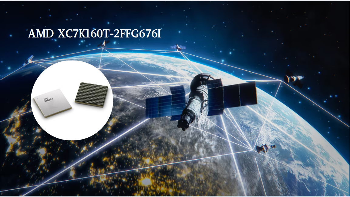
The AMD XC7K160T - 2FFG676I, a member of the Kintex - 7 FPGA family, offers a compelling combination of features. It boasts a rich array of logic resources, allowing for the implementation of intricate digital designs, making it suitable for complex tasks like AI algorithm processing and 5G signal handling. Its low - power consumption design ensures energy - efficient operation, ideal for battery - powered devices and large - scale data centers. With high - speed signal processing capabilities, it can manage rapid data streams, crucial for 5G communication and other high - speed applications. The device’s programmability provides great flexibility, enabling users to customize it for diverse needs, from consumer electronics to industrial control. Its support for multiple standards and excellent parallel processing performance further enhance its versatility, while reliable operation guarantees consistent performance across various environments.
AMD XC7K160T-2FFG676I's Features
The AMD XC7K160T - 2FFG676I, as a part of the Kintex - 7 series Field Programmable Gate Array (FPGA), has the following features:
- High Logic Resource Abundance: It comes with a large number of logic elements, flip-flops, and other resources. These abundant logic resources enable it to implement complex digital circuits and algorithms, such as those required for neural network models in artificial intelligence applications, allowing for the processing of multiple tasks simultaneously and handling of large amounts of data.
- Low Power Consumption: Incorporates advanced semiconductor manufacturing processes and power management techniques. It can operate with relatively low power consumption while still maintaining good performance. This makes it suitable for applications where power consumption is a critical factor, such as in battery-powered devices or large-scale data centers where energy efficiency is highly valued.
- High-Speed Signal Processing Capability: Capable of handling high-speed data streams. It can perform operations like high-speed data acquisition, processing, and transmission. In 5G communication systems, it can support the processing of high-frequency signals, including baseband processing, intermediate frequency processing, and radio frequency processing, and meet the requirements of 5G for fast data transmission and complex signal processing.
- Flexibility and Programmability: Being an FPGA, it offers great flexibility. Users can program it according to their specific application needs, reconfiguring the internal logic and connections. This feature allows it to be quickly adapted to different application scenarios, whether in consumer electronics for functions like image signal processing in LED backlit displays or in industrial control for implementing various control algorithms.
- Compatibility with Multiple Standards: Supports various communication and interface standards. In wireless communication, it can work with standards such as LTE and Wi-Fi, enabling seamless integration into different communication systems. In industrial control, it can interface with other devices and systems according to relevant industrial communication protocols, facilitating the construction of complex industrial automation systems.
- High Performance in Parallel Processing: Can execute multiple operations in parallel. This parallel processing ability significantly improves its processing efficiency, especially in applications that require simultaneous handling of multiple data streams, such as in cloud computing for data encryption and decryption, network packet processing, and distributed storage system operations.
- Reliability and Stability: Built with robust semiconductor technology and design, it can operate stably in different environments. It can withstand certain levels of temperature, humidity, and electrical interference, ensuring reliable performance in various application scenarios, whether in harsh industrial environments or complex medical equipment systems.
Advantages and Disadvantages of the XC7K160 FPGA
The XC7K160 FPGA, a member of the Kintex - 7 family by AMD (formerly Xilinx), has several advantages and disadvantages, which are detailed as follows:
Advantages
- High Performance
- It offers a substantial number of logic resources, including 162,240 logic cells. This allows for the implementation of complex digital circuits, making it suitable for applications requiring high - level processing power, such as digital signal processing, image processing, and high - speed data communication.
- The device supports high - speed serial transceivers, enabling data rates of up to 12.5 Gbps. This makes it well - suited for applications that demand high - speed data transmission, such as Ethernet, PCI - Express, and optical communication.
- Low Power Consumption
- The Kintex - 7 family uses a 28 - nm High - K metal - gate process, which helps to reduce power consumption. The XC7K160, in particular, is designed to operate efficiently, making it suitable for applications where power efficiency is critical, such as portable devices and energy - conscious data centers.
- It features advanced power - management capabilities, including dynamic voltage and frequency scaling (DVFS). This allows the FPGA to adjust its power consumption based on the actual workload, further optimizing energy efficiency.
- Rich Peripherals and Interfaces
- It comes with a variety of built - in peripherals, such as block RAM, DSP slices, and PCI - Express interfaces. The 36 - kb dual - port block RAM with built - in FIFO logic provides on - chip data storage and buffering, while the DSP slices are optimized for digital signal processing tasks.
- The integrated PCI - Express block supports up to x8 Gen 3 endpoint and root port designs, enabling high - speed communication with other devices in a system. Additionally, it offers a wide range of other interfaces, including GPIO, Ethernet, and USB, facilitating easy integration with various external components.
Disadvantages
- Cost
- FPGAs, in general, tend to be more expensive than other off - the - shelf integrated circuits. The XC7K160 is no exception. Its high - performance capabilities and advanced features come at a cost, which may make it less attractive for cost - sensitive applications.
- The cost of development tools and licenses associated with the XC7K160 can also add to the overall expense. The Vivado design suite, which is required for programming and configuring the FPGA, may have a significant licensing cost, especially for commercial use.
- Complexity
- Programming and configuring an FPGA can be a complex and time - consuming process. The XC7K160, with its large number of logic resources and advanced features, requires a high level of expertise in digital design and FPGA programming. Designers need to have a good understanding of HDL (Hardware Description Language), such as VHDL or Verilog, as well as the specific tools and techniques for FPGA development.
- The development process often involves multiple steps, including design entry, synthesis, place and route, and verification. Each step requires careful attention and can be prone to errors. Debugging and optimizing the design can also be challenging, especially for complex applications.
- Limited On - Chip Memory
- While the XC7K160 has a certain amount of on - chip memory in the form of block RAM, it may not be sufficient for some applications that require large amounts of data storage. Compared to dedicated memory chips, the on - chip memory in FPGAs is relatively limited.
- If an application requires a large amount of data to be stored and accessed quickly, additional external memory may be needed. This can increase the complexity and cost of the overall system design.
AMD XC7K160T-2FFG676I's Applications
The AMD XC7K160T - 2FFG676I is a Field Programmable Gate Array (FPGA) of the Kintex - 7 series, featuring high cost-effectiveness, low power consumption, etc., and can be applied in multiple fields as follows:
Artificial Intelligence: This chip has abundant logic resources and high-speed signal processing capabilities, and can be used to construct neural network models in artificial intelligence algorithms, and accelerate tasks such as image recognition, speech recognition, and natural language processing.
5G Technology: In the 5G communication system, it can be used to achieve functions such as baseband processing, intermediate frequency processing, and radio frequency processing, and support high-speed data transmission and complex signal processing algorithms in the 5G network, such as Digital Pre-Distortion (DPD), channel encoding and decoding, etc.
Cloud Computing: It is suitable for cloud computing data centers and can serve as a hardware acceleration engine to provide efficient hardware support for data encryption and decryption, network packet processing, distributed storage systems, etc. in cloud computing, and improve the performance and efficiency of the cloud computing platform.
Consumer Electronics: It can be used in consumer electronic products such as LED backlit flat panel displays and 3D TVs to achieve functions such as image signal processing, video decoding, and display control, and enhance the display effect and user experience.
Wireless Communication: It can be applied to wireless communication base stations and terminal devices to achieve functions such as modulation and demodulation of wireless signals, channel encoding and decoding, signal filtering, etc., and support various wireless communication standards, such as LTE, Wi-Fi, etc.
Industrial Control: It can be used in industrial automation control systems to achieve functions such as logical control, motion control, and process control, collect, process, and control various signals in the industrial production process, and improve the efficiency and quality of industrial production.
Internet of Things: In Internet of Things devices, it can serve as a core processor to achieve sensor data collection, processing, and transmission, support communication and collaborative work between Internet of Things devices, and provide powerful computing and control capabilities for Internet of Things applications.
Medical Equipment: It can be applied to medical imaging equipment, medical monitoring equipment, and other medical devices to achieve functions such as image reconstruction, signal processing, and data transmission, improve the performance and accuracy of medical equipment, and provide strong support for medical diagnosis and treatment.
AMD XC7K160T-2FFG676I's Attributes
| Product Category |
FPGA - Field Programmable Gate Array |
RoHS |
Details |
| Series |
XC7K160T |
Number of Logic Elements |
162240 LE |
| Adaptive Logic Modules - ALMs |
25350 ALM |
Embedded Memory |
11.43 Mbit |
| Number of I/Os |
400 I/O |
Supply Voltage - Min |
970 mV |
| Supply Voltage - Max |
1.03 V |
Minimum Operating Temperature |
- 40 C |
| Maximum Operating Temperature |
+ 100 C |
Data Rate |
12.5 Gb/s |
| Number of Transceivers |
8 Transceiver |
Mounting Style |
SMD/SMT |
| Package / Case |
FCBGA-676 |
Brand |
Xilinx |
| Distributed RAM |
2188 kbit |
Embedded Block RAM - EBR |
11700 kbit |
| Maximum Operating Frequency |
640 MHz |
Moisture Sensitive |
Yes |
| Number of Logic Array Blocks - LABs |
12675 LAB |
Operating Supply Voltage |
1.2 V to 3.3 V |
| Product Type |
FPGA - Field Programmable Gate Array |
Factory Pack Quantity |
1 |
| Subcategory |
Programmable Logic ICs |
Tradename |
Kintex |
| Unit Weight |
3.506996 oz |
|
|
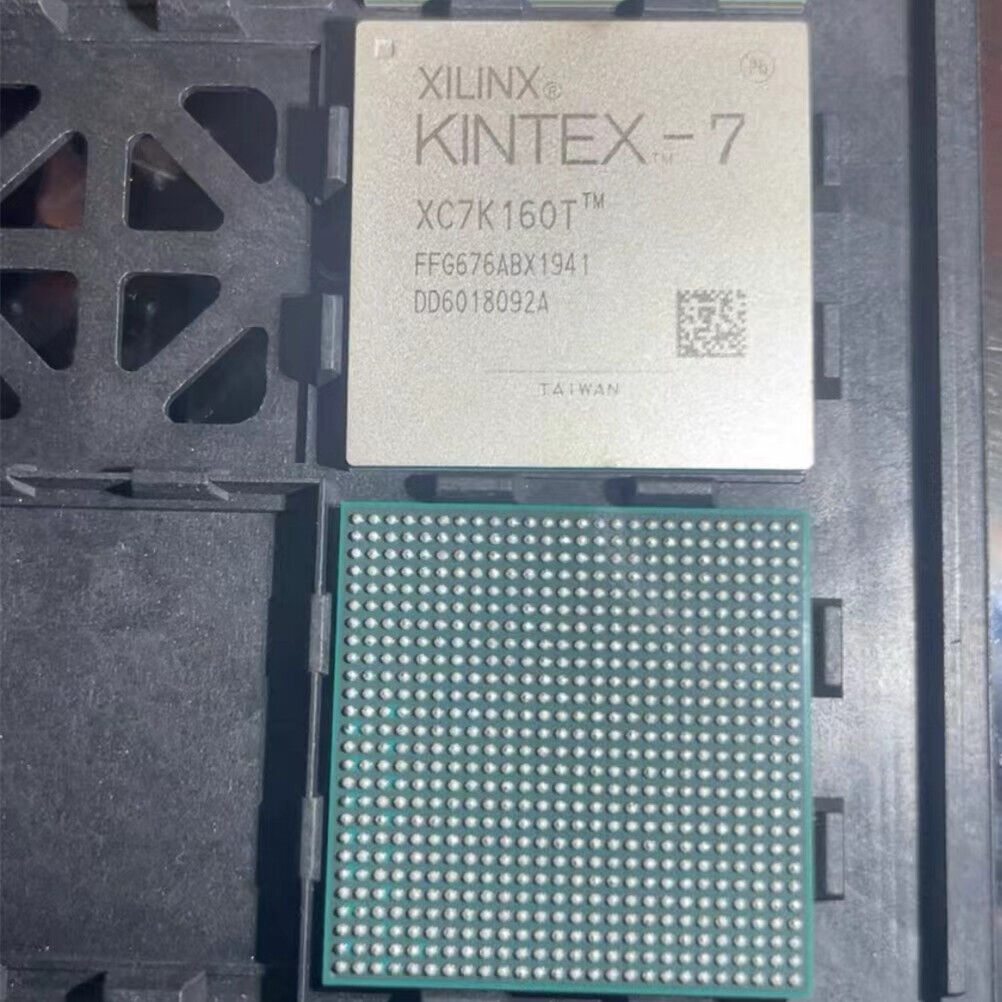
AMD XC7K160T-2FFG676I's Pinout and Configuration
The pinout and configuration of the AMD XC7K160T - 2FFG676I are crucial aspects for understanding and using this FPGA device.
Pinout
- The XC7K160T - 2FFG676I is a 676 - pin device1. It has 400 maximum user I/Os, which provide flexible connections for various external devices and signals. These I/O pins can be configured to support different interfaces and protocols, such as high - speed serial interfaces like GTX transceivers for high - speed data transmission, and parallel interfaces for connecting to other components like memory or peripheral devices.
- There are also specific pins dedicated to power supply and ground, ensuring stable power supply to the device. In addition, there are pins for clock signals, which are essential for synchronizing the internal operations of the FPGA.
Configuration
- The device is configured through programming, which can be done using tools like the Vivado design suite provided by AMD (formerly Xilinx). The configuration data determines the functionality and behavior of the FPGA, including how the logic cells, memory blocks, and interconnects are utilized.
- The XC7K160T - 2FFG676I has a rich set of configurable features. It has 162,240 logic cells that can be used to implement complex digital circuits. The 36 - kb dual - port block RAM with built - in FIFO logic is available for on - chip data buffering, and the DSP slices with 25x18 multiplier, 48 - bit accumulator, and pre - adder are suitable for high - performance filtering and other digital signal processing tasks. Moreover, the integrated PCIe block supports up to x8 Gen 3 endpoint and root port designs, enabling high - speed communication with other devices in a system.
AMD XC7K160T-2FFG676I's Category- FPGAs
Field Programmable Gate Arrays (FPGAs) are versatile integrated circuits that have revolutionized the electronics industry. Unlike traditional fixed - function chips, FPGAs can be programmed and reprogrammed by designers after manufacturing, offering unparalleled flexibility. This programmability allows them to adapt to a wide range of applications, from high - performance computing and digital signal processing to networking and embedded systems. FPGAs consist of an array of logic cells, memory blocks, and programmable interconnections. These elements can be configured to implement complex digital circuits, enabling users to quickly prototype and deploy custom - designed solutions. They are highly efficient in handling parallel processing tasks, making them ideal for applications that require processing multiple data streams simultaneously, such as image and video processing, cryptocurrency mining, and artificial intelligence acceleration. One of the significant advantages of FPGAs is their ability to offer a balance between performance and power consumption. They can be optimized to meet specific power requirements while still delivering high - speed operation, making them suitable for both power - constrained mobile devices and high - performance data centers.
Among the many FPGA offerings, the AMD XC7K160T - 2FFG676I from the Kintex - 7 series stands out. It combines the general benefits of FPGAs with its own unique features. With abundant logic resources, it can handle complex algorithms and designs. Its low - power consumption and high - speed processing capabilities make it a top choice for applications in 5G communication, cloud computing, and industrial control, further demonstrating the remarkable potential and adaptability of FPGAs in modern technology.
XC7K160T-2FFG676I's Manufacturer-AMD
AMD has achieved remarkable success in the field of FPGAs (Field Programmable Gate Arrays), boasting profound technical accumulation and extensive market influence. In the nearly 40 years since it entered the FPGA field, AMD has launched a diverse range of product series through continuous innovation and optimization, covering various application scenarios with requirements ranging from low-cost and low-power consumption to high-performance and high-integration. The breadth and depth of its product line enable customers from different industries to find solutions that suit their own needs. For example, in the aerospace field, AMD's FPGA products assist in building high-precision satellite communication and navigation systems; in the medical device field, they provide core computing support for advanced medical imaging and diagnostic equipment.
In terms of technological innovation, AMD actively introduces cutting-edge manufacturing processes. Take the Spartan UltraScale+ series as an example. This series is built based on the mature 16nm FinFET process. Compared with its previous products using the 28nm process, the total power consumption has been significantly reduced by up to 30%, and the power consumption of interface connections can be reduced by up to 60%. At the same time, the architecture performance has been increased by 1.9 times, and there have been substantial growth in key indicators such as the number of I/O, memory controller bandwidth, and PCIe bandwidth. In addition, AMD continuously strengthens the security features of its products. The Spartan UltraScale+ series supports post-quantum cryptography technology and has algorithms approved by the NIST (National Institute of Standards and Technology), which can effectively resist cyberattacks. The physical unclonable function assigns a unique fingerprint to each device, further enhancing security.
In terms of market performance, AMD's FPGA products have a shipment volume of billions and are widely applied in multiple industries. The Spartan FPGA series, since its launch in 1998, has gone through six generations of upgrades and has been used in major projects such as life-saving automatic defibrillators, Mars exploration instruments, and the particle accelerator of the European Organization for Nuclear Research (CERN). AMD also provides convenient and efficient design environments for hardware and software designers through the Vivado design suite and the Vitis unified software platform, reducing the development difficulty and improving the design efficiency. Moreover, AMD promises that its FPGA products have an extremely long life cycle. The products of the 7 series can be extended until 2040, and the UltraScale+ products can last until 2045, providing customers with long-term and stable technical support and guarantee.
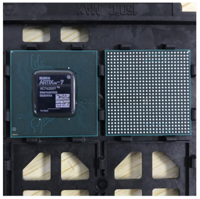
XC7K160T-2FFG676C alternative parts: XC7A200T-2FBG676I
|
Hide Shared Attributes
|
|
|
|
Part Number
|
XC7K160T-2FFG676C +BOM
|
XC7A200T-2FBG676I +BOM
|
|
Manufacturer:
|
Xilinx Inc.
|
Xilinx Inc.
|
|
Description:
|
IC FPGA 400 I/O 676FCBGA
|
IC FPGA ARTIX7 400 I/O 676FCBGA
|
|
Factory Lead Time:
|
10 Weeks
|
10 Weeks
|
|
Contact Plating:
|
Copper, Silver, Tin
|
Copper, Silver, Tin
|
|
Mounting Type:
|
Surface Mount
|
Surface Mount
|
|
Package / Case:
|
676-BBGA, FCBGA
|
676-BBGA, FCBGA
|
|
Surface Mount:
|
YES
|
YES
|
|
Number of Pins:
|
676
|
676
|
|
Number of I/Os:
|
400
|
400
|
|
Operating Temperature:
|
0°C~85°C TJ
|
-40°C~100°C TJ
|
|
Packaging:
|
Tray
|
Tray
|
|
Series:
|
Kintex®-7
|
Artix-7
|
|
Published:
|
2010
|
2009
|
|
JESD-609 Code:
|
e1
|
e1
|
|
Pbfree Code:
|
yes
|
yes
|
|
Part Status:
|
Active
|
Active
|
|
Moisture Sensitivity Level (MSL):
|
4 (72 Hours)
|
4 (72 Hours)
|
|
Number of Terminations:
|
676
|
676
|
|
ECCN Code:
|
3A991.D
|
3A991.D
|
|
Terminal Finish:
|
Tin/Silver/Copper (Sn96.5Ag3.0Cu0.5)
|
Tin/Silver/Copper (Sn96.5Ag3.0Cu0.5)
|
|
HTS Code:
|
8542.39.00.01
|
8542.39.00.01
|
|
Voltage - Supply:
|
0.97V~1.03V
|
0.95V~1.05V
|
|
Terminal Position:
|
BOTTOM
|
BOTTOM
|
|
Terminal Form:
|
BALL
|
BALL
|
|
Supply Voltage:
|
1V
|
1V
|
|
Terminal Pitch:
|
1mm
|
1mm
|
|
Base Part Number:
|
XC7K160
|
XC7A200T
|
|
Pin Count:
|
676
|
676
|
|
Number of Outputs:
|
400
|
400
|
|
Power Supplies:
|
11.83.3V
|
1V
|
|
RAM Size:
|
1.4MB
|
1.6MB
|
|
Clock Frequency:
|
1818MHz
|
1286MHz
|
|
Programmable Logic Type:
|
FIELD PROGRAMMABLE GATE ARRAY
|
FIELD PROGRAMMABLE GATE ARRAY
|
|
Number of Logic Elements/Cells:
|
162240
|
215360
|
|
Total RAM Bits:
|
11980800
|
13455360
|
|
Number of LABs/CLBs:
|
12675
|
16825
|
|
Speed Grade:
|
-2
|
-2
|
|
Number of Registers:
|
202800
|
269200
|
|
Combinatorial Delay of a CLB-Max:
|
0.61 ns
|
1.05 ns
|
|
Length:
|
27mm
|
27mm
|
|
Height Seated (Max):
|
3.37mm
|
2.54mm
|
|
Width:
|
27mm
|
27mm
|
|
Radiation Hardening:
|
No
|
-
|
|
RoHS Status:
|
ROHS3 Compliant
|
ROHS3 Compliant
|
|
Memory Types:
|
-
|
DDR3
|
|
Peak Reflow Temperature (Cel):
|
-
|
NOT SPECIFIED
|
|
Time@Peak Reflow Temperature-Max (s):
|
-
|
NOT SPECIFIED
|
|
Qualification Status:
|
-
|
Not Qualified
|
|
Memory Size:
|
-
|
1GB
|
WlS Electronic holds a large inventory of AMD XC7K160T-2FFG676I. We assure you that these are genuine and brand-new components, directly sourced from AMD. If needed, we can provide quality test reports for the XC7K160T-2FFG676I. To obtain a quotation, just fill in the desired quantity, your contact name, and your email address in the quick quotation form on the right. Our sales representatives will get in touch with you within 12 hours. You can contact us online at any time, or send an email to: SALES@WLSCHIP.COM.


