The STMicroelectronics STM32F101VBT6 is a medium-density ARM Cortex-M3 microcontroller designed for embedded applications. It features a 32-bit Cortex-M3 core running at up to 36 MHz, offering 1.25 DMIPS/MHz performance with 0 wait-state memory access, 128 KB Flash, and 16 KB SRAM. Equipped with versatile peripherals, it includes 3 x 16-bit general-purpose timers for PWM and input capture, a 12-bit ADC with 16 channels (1 µs conversion time), 2 x I²C (SMBus/PMBus), 3 x USART (supporting LIN, IrDA), and 2 x SPI (up to 18 Mbit/s). Low-power modes—Sleep, Stop, and Standby—ensure energy efficiency, with VBAT supporting RTC and backup registers during power loss. The LQFP100 package provides 80 high-speed I/Os, most with 5V tolerance, mappable to 16 external interrupts. Debugging is enabled via SWD and JTAG interfaces. Operating over 2.0–3.6V and –40°C to +85°C, it suits industrial, consumer, and medical applications, balancing performance, integration, and power efficiency.
STMicroelectronics STM32F101VBT6's Features
The STM32F101VBT6, developed by STMicroelectronics, is a medium-density ARM® Cortex®-M3 microcontroller (MCU) renowned for its high performance, rich peripherals, and low-power capabilities, making it suitable for a wide range of embedded applications. Below is a summary of its core features:
1. Core and Performance
- Processor: 32-bit ARM Cortex-M3 core with a maximum operating frequency of 36 MHz, delivering 1.25 DMIPS/MHz performance (Dhrystone 2.1 benchmark, 0 wait-state memory access). Supports single-cycle multiplication and hardware division for efficient computation in intensive tasks.
- Memory:
- Flash Storage: 128 KB (designated by "B" in the part number) for program and data storage.
- SRAM: 16 KB (matched with 128 KB Flash), enabling zero-wait-state access to accelerate data processing.
2. Clock and Power Management
- Clock Sources:
- External High-Speed Clock (HSE): 4–16 MHz crystal/ceramic resonator or external clock input.
- Internal High-Speed RC (HSI): 8 MHz factory-trimmed RC for fast startup.
- Internal Low-Speed RC (LSI): 40 kHz, used for low-power mode clocking.
- 32.768 kHz Low-Speed External Clock (LSE): Provides precise timing for the Real-Time Clock (RTC).
- PLL: Frequency multiplier supporting up to 36 MHz system clock.
- Power Supply:
- Main Power (VDD): 2.0–3.6 V, powering I/Os and the core.
- Analog Power (VDDA): 2.0–3.6 V (minimum 2.4 V when using the ADC).
- Backup Power (VBAT): 1.8–3.6 V, sustaining RTC and backup registers when the main power is off.
- Low-Power Modes:
- Sleep Mode: CPU stops, peripherals remain active, wakeable by interrupts/events.
- Stop Mode: Minimum power consumption, retains SRAM and registers; clocks halted, wakeable via EXTI, RTC, etc.
- Standby Mode: Lowest power consumption, voltage regulator off (only RTC and backup registers retained), wakeable by external reset or RTC alarm.
3. Peripherals and Interfaces
- Timers:
- 3 x 16-bit General-Purpose Timers (TIM2, TIM3, TIM4): 4 channels each, supporting input capture, output compare, PWM generation (e.g., motor control, waveform generation).
- 2 x Watchdog Timers: Independent Watchdog (IWDG) and Window Watchdog (WWDG) for system robustness.
- SysTick Timer: 24-bit downcounter for OS timing or delay functions.
- Communication Interfaces:
- USART: 3 USARTs supporting ISO 7816, LIN, IrDA, and modem control, up to 2.25 Mbit/s.
- SPI: 2 SPIs with up to 18 Mbit/s, supporting full-duplex/half-duplex, master/slave modes, and compatibility with SD cards/MMC.
- I²C: 2 I²C interfaces supporting SMBus/PMBus, multimaster mode, and standard/fast modes (100/400 kHz).
- DMA Controller: 7-channel DMA for data transfer between peripherals (e.g., ADC, SPI, USART) and memory, reducing CPU load.
- Analog Peripherals:
- 12-bit ADC: 16 channels, 1 µs conversion time, supporting single-ended/differential inputs with an internal temperature sensor (ADC_IN16), conversion range 0–3.6 V.
- Analog Watchdog: Triggers interrupts when converted voltage exceeds programmed thresholds.
- GPIOs:
- Up to 80 high-speed I/O pins (LQFP100 package), almost all 5V tolerant, mappable to 16 external interrupt lines. Supports push-pull/open-drain outputs and pull-up/pull-down input configurations.
4. Debugging and Security
- Debug Interfaces: Supports Serial Wire Debug (SWD) and JTAG for easy code download and debugging.
- Security Features: 96-bit unique ID and CRC calculation unit for data integrity verification (e.g., Flash memory validation).
5. Packaging and Specifications
- Package: LQFP100 (14x14 mm, 100 pins), compatible with the industrial temperature range (-40°C to +85°C).
- Compatibility: Pin-to-pin and software compatibility with the STM32F101xx family, enabling seamless migration to different density models (low/high density).
STMicroelectronics STM32F101VBT6's Applications
The STM32F101VBT6, a medium-density ARM Cortex-M3 microcontroller from STMicroelectronics, is suited for a wide range of embedded applications due to its high performance, rich peripherals, and low-power characteristics. Below is an analysis of its core application areas and advantages:
1. Industrial Control and Automation
Application Scenarios
PLC (Programmable Logic Controllers), industrial inverters, motor control, sensor data acquisition
Core Advantages
Multi-Timers and Communication Interfaces:
3 x 16-bit general-purpose timers (TIM2/TIM3/TIM4) support PWM generation and input capture, ideal for motor speed control and stepper motor control.
2 x SPI (18 Mbit/s), 2 x I²C (supporting SMBus/PMBus), and 3 x USART (supporting LIN/IrDA/Modem) meet requirements for industrial buses (e.g., MODBUS, CAN-derived protocols).
High-Precision ADC:
12-bit ADC (16 channels, 1 µs conversion time) combined with an internal temperature sensor enables industrial sensor data acquisition (e.g., voltage, current, temperature monitoring).
Reliability:
Industrial temperature range of -40°C to +85°C, with hardware watchdogs (IWDG/WWDG) to ensure stable operation in harsh environments.
2. Consumer Electronics and Handheld Devices
Application Scenarios
Smart home devices (e.g., smart sockets, thermostats), handheld scanners, portable medical devices (glucose meters, blood pressure monitors)
Core Advantages
Low-Power Design:
Sleep, Stop, and Standby modes significantly reduce energy consumption, suitable for battery-powered devices (e.g., Bluetooth remotes, wearables).
VBAT backup power supports the RTC (real-time clock) to maintain time and configuration data during VDD power loss.
Flexible GPIO and Interfaces:
80 high-speed I/O pins (most with 5V tolerance) support custom input/output for buttons, LED displays, and touch sensors.
USART and I²C are compatible with peripherals like Bluetooth modules and LCD drivers.
Cost-Effectiveness:
Balanced performance and integration reduce hardware design complexity and costs.
3. Medical Devices and Portable Instruments
Application Scenarios
Medical monitors, portable diagnostic devices, health monitoring equipment
Core Advantages
High-Precision Analog Processing:
12-bit ADC supports biometric signal acquisition (e.g., heart rate, body temperature), with an internal temperature sensor simplifying hardware design.
DMA controller efficiently handles continuous data transfer, reducing CPU load.
Reliable Communication:
USART and I²C support common medical device protocols (e.g., UART-to-USB, I²C-connected sensor modules) for stable data transmission.
Low Power and Stability:
Low-power modes extend battery life, and the industrial temperature range adapts to variable environments.
4. IoT and Edge Computing
Application Scenarios
IoT sensor nodes, gateway edge devices, environmental monitoring terminals
Core Advantages
Multi-Communication Interfaces:
SPI/USART/I²C support diverse sensors (e.g., Wi-Fi, Zigbee, LoRa modules) for flexible IoT ecosystem integration.
7-channel DMA enables efficient bulk sensor data transfer.
Low Power and Wake-Up Mechanisms:
Standby mode current as low as µA levels, paired with external interrupts (EXTI) for fast wake-up, suitable for long-running wireless sensor nodes.
Hardware Security:
96-bit unique ID and CRC check unit ensure data transmission and storage integrity.
5. Computer Peripherals and Interface Devices
Application Scenarios
USB peripherals (e.g., keyboards, mice, printers), industrial serial-to-interface converters, embedded gateways
Core Advantages
High-Speed Communication Support:
USART supports IrDA and modem control for legacy serial devices.
SPI interface is compatible with SD cards and peripheral controllers for storage and function expansion.
Compatibility:
5V-tolerant GPIOs connect directly to external devices, reducing level-conversion circuits.
SWD/JTAG debug interfaces simplify development and debugging.
6. Embedded Control and Instruments
Application Scenarios
Printers, scanners, industrial meters, smart energy meters
Core Advantages
Timers and PWM:
3 timers support multi-channel PWM output for motor or peripheral control.
Hardware division and single-cycle multiplication accelerate data processing for real-time control.
System-Level Integration:
Nested Vector Interrupt Controller (NVIC) enables low-latency interrupt response for multi-task real-time processing.
Boot modes support system memory boot for easy firmware upgrades.
7. Automotive Electronics and In-Vehicle Devices
Application Scenarios
In-vehicle sensor nodes, body control modules (BCM), in-vehicle communication devices
Core Advantages
Wide Temperature Range and Reliability:
Operating temperature of -40°C to +85°C adapts to in-vehicle environments, with hardware watchdogs and voltage monitoring (PVD) for system stability.
Bus Compatibility:
USART supports LIN protocol for low-speed in-vehicle networks.
SPI/I²C connects to in-vehicle sensors (e.g., temperature, pressure sensors).
STMicroelectronics STM32F101VBT6's Attributes
| Operating Range |
Industrial |
Supply Voltage Min Volt |
2.0 |
| Supply Voltage Max Volt |
3.6 |
Operating Temp Min Celsius |
-40.0 |
| Operating Temp Max Celsius |
85.0 |
Core |
Arm Cortex-M3 |
| ECCN US |
3A991.a.2 |
ECCN EU |
NEC |
| Packing Type |
Tray |
RoHs compliant |
Ecopack2 |
| Grade |
Industrial |
Package Name |
LQFP 100 14x14x1.4 mm |

STMicroelectronics STM32F101VBT6's Symbol, Footprint and 3D Model
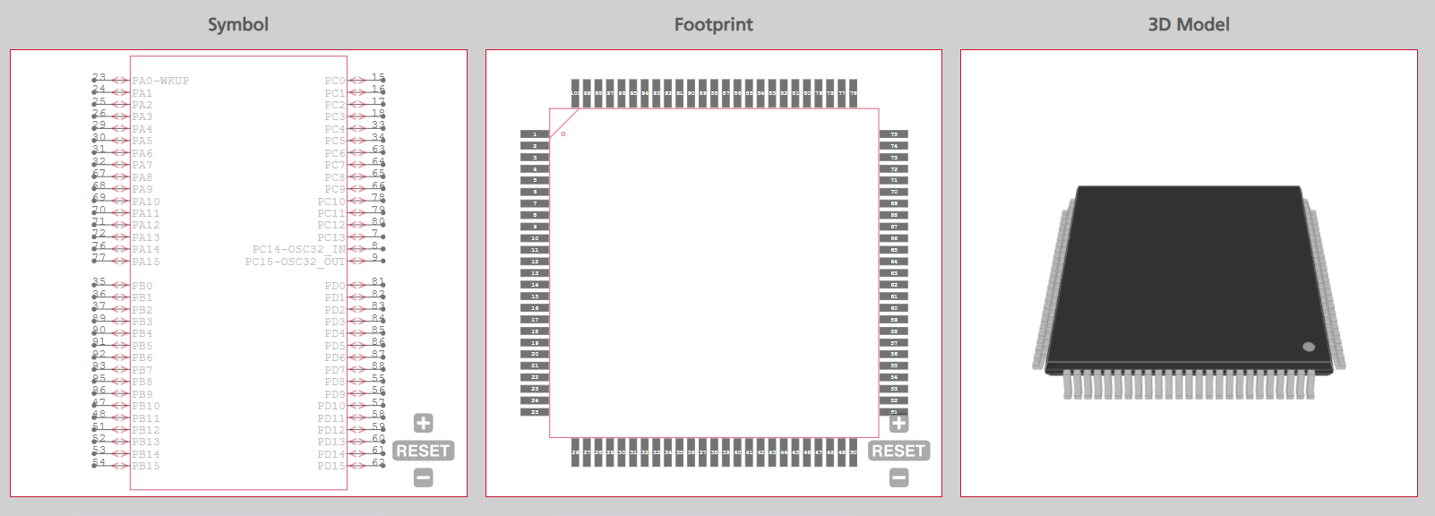
Pinout:
The STM32F101VBT6 belongs to the STM32F101xB series and uses an LQFP100 package (100 pins, 14x14mm). Below is its main pin configuration and functional classification:
I. Power and Ground Pins
| Pin Name |
Function Description |
| VDD_1~VDD_5 |
Main power input (2.0–3.6V). Multiple power pins supply different regions; decoupling capacitors (e.g., 100nF and 4.7μF) are required. |
| VSS_1~VSS_5 |
Ground pins corresponding to VDD pins to ensure power stability. |
| VDDA |
Analog power input (2.0–3.6V), supplying analog peripherals like ADC and PLL. Must share ground with VDD. |
| VSSA |
Analog ground, corresponding to VDDA. |
| VBAT |
Backup power input (1.8–3.6V), powering RTC and backup registers to maintain time/data when VDD is off. |
II. Clock and Reset Pins
| Pin Name |
Function Description |
| OSC_IN (PD0) |
External high-speed clock input (4–16MHz), supporting crystal/ceramic resonators or external clock sources. |
| OSC_OUT (PD1) |
External high-speed clock output, used with OSC_IN. |
| OSC32_IN (PC14) |
External low-speed clock input (32.768kHz), providing timing for RTC. |
| OSC32_OUT (PC15) |
External low-speed clock output, used with OSC32_IN. |
| NRST |
Reset input pin (active low), with an internal pull-up resistor (≈40kΩ). An external reset circuit can be connected. |
III. GPIO Pins
General-Purpose Input/Output Ports
- PA0~PA15: 32 GPIOs supporting input/output and alternate functions (e.g., USART, SPI, ADC).
Example: PA0 can serve as WKUP Wake-up Pin, USART2_CTS, or ADC_IN0.
- PB0~PB15: 32 GPIOs, with some pins multiplexed for I2C, SPI, USART, etc.
Example: PB6 (I2C1_SCL), PB7 (I2C1_SDA), PB10 (I2C2_SCL/USART3_TX).
- PC0~PC15: 32 GPIOs, where PC13~PC15 are for RTC/Tamper with limited load capability (max 3mA, speed ≤2MHz).
- PD0~PD15: 32 GPIOs, with some pins used for USART and timers (e.g., PD6 for USART2_RX).
- PE0~PE15: 32 GPIOs, with some pins for trace debugging (e.g., PE2~PE5 for TRACED0~TRACED3).
Special Functions
- BOOT0 (PB2): Boot mode selection pin (high: system memory boot; low: user Flash boot).
- PC13 (TAMPER-RTC): Tamper detection/RTC function, supporting reset or wake-up.
IV. Peripheral Interface Pins
Communication Interfaces
| Interface |
Pin Assignment |
| USART1 |
PA9 (TX), PA10 (RX), PA11 (CTS), PA12 (RTS), PA8 (CK). |
| USART2 |
PA2 (TX), PA3 (RX), PA0 (CTS), PA1 (RTS), PA4 (CK). |
| USART3 |
PB10 (TX), PB11 (RX), PC10 (CK), PD8 (CTS), PD9 (RTS). |
| I2C1 |
PB6 (SCL), PB7 (SDA), supporting SMBus/PMBus. |
| I2C2 |
PB10 (SCL), PB11 (SDA), supporting multi-master mode. |
| SPI1 |
PA5 (SCK), PA6 (MISO), PA7 (MOSI), PA4 (NSS), up to 18Mbit/s. |
| SPI2 |
PB13 (SCK), PB14 (MISO), PB15 (MOSI), PB12 (NSS). |
Timers and ADC
| Function |
Pin Assignment |
| General Timers |
TIM2 (PA0~PA3), TIM3 (PA6/PA7, PB0/PB1), TIM4 (PB6~PB9). |
| ADC Channels |
PA0~PA7 (ADC_IN0~IN7), PB0/PB1 (ADC_IN8/IN9), PC0~PC5 (ADC_IN10~IN15). |
| Temperature Sensor |
ADC_IN16 (internally connected, no external pin required). |
V. Debug Interface Pins
| Pin Name |
Function Description |
| SWDIO (PA13) |
Serial Wire Debug data I/O, supporting SWD debug interface. |
| SWCLK (PA14) |
Serial Wire Debug clock, used with SWDIO. |
| JTDI (PA15) |
JTAG data input (multiplexed with TIM2_CH1_ETR). |
| JTDO (PB3) |
JTAG data output (multiplexed with TRACESWO). |
| JTMS/SWDIO |
JTAG mode select (multiplexed with SWDIO). |
| JTCK/SWCLK |
JTAG clock (multiplexed with SWCLK). |
VI. Other Key Pins
| Pin Name |
Function Description |
| VREF+ |
Positive ADC reference voltage input (2.4–3.6V, exclusive to 100-pin package). |
| VREF- |
Negative ADC reference voltage input (usually grounded). |
| VBAT |
Backup power to support RTC and backup registers when the main power is off. |
Pin Layout Overview (LQFP100)
- Top-left: PE port (PE0~PE15), VBAT, OSC32_IN/OUT.
- Top-right: PD port (PD0~PD15), OSC_IN/OUT, NRST.
- Bottom: PA port (PA0~PA15), VDDA/VSSA, VREF±.
- Left side: PB port (PB0~PB15), BOOT0, power pins (VDD_1~VSS_1).
- Right side: PC port (PC0~PC15), timer/ADC channels.
Key Notes
- Alternate Functions: Most GPIOs support peripheral multiplexing, configured via registers (e.g., AFIO remapping).
- 5V Tolerance: Most GPIOs are 5V-tolerant (marked with "FT"), except PC13~PC15.
- Power Configuration: VDDA must share ground with VDD; analog sections require separate decoupling (10nF + 1μF).
- Debug Interface: The SWD interface only needs SWDIO and SWCLK, saving more pins than JTAG.
STMicroelectronics STM32F101VBT6's Category-Microcontrollers
Microcontrollers (MCUs) serve as the core of embedded systems, integrating a central processing unit (CPU), memory, peripheral interfaces, and various functional modules. Widely used in industrial control, consumer electronics, medical devices, the Internet of Things (IoT), and other fields, their design emphasizes low power consumption, high integration, and real-time performance to enable efficient control in resource-constrained environments. Typical microcontrollers are equipped with timers, ADCs, communication interfaces (such as UART, SPI, I²C), and other components, supporting real-time data processing and device interconnection to meet diverse application needs.
The ARM Cortex-M series cores have become one of the mainstream choices due to their balance of high performance and low power consumption. For example, the STM32F101VBT6, a medium-density microcontroller from STMicroelectronics, features a 32-bit Cortex-M3 core with a maximum clock speed of 36 MHz, 128 KB of Flash memory, and 16 KB of SRAM. It supports single-cycle multiplication and hardware division, ensuring efficient arithmetic operations. Its rich peripherals include 3 general-purpose timers, a 12-bit ADC (16 channels), 2 SPI interfaces, 3 USARTs, and 2 I²C interfaces, adapting to tasks such as sensor data acquisition and communication protocol processing. The low-power design includes Sleep, Stop, and Standby modes, combined with VBAT backup power, making it suitable for battery-powered devices.
Housed in an LQFP100 package, the STM32F101VBT6 supports 80 high-speed GPIOs (most with 5V tolerance) and operates within an industrial temperature range of -40°C to +85°C, balancing flexibility and reliability. Its Nested Vector Interrupt Controller (NVIC) and DMA controller enhance real-time response capabilities, making it suitable for applications such as industrial automation, smart devices, and portable instruments. With mature ecosystem support and pin compatibility, this device becomes an ideal choice for embedded development, balancing performance, cost, and power consumption effectively.
STM32F101VBT6's Manufacturer-STMicroelectronics
STMicroelectronics has established itself as a global leader in microcontroller (MCU) innovation, driving advancements in embedded systems with its iconic STM32 family. Central to its success is the integration of high-performance ARM® Cortex®-M cores, such as the Cortex-M3 in the STM32F101xB series, delivering up to 36 MHz operation, 1.25 DMIPS/MHz efficiency, and hardware acceleration for critical tasks like single-cycle multiplication. This architecture balances power efficiency with robust processing, featuring low-power modes—Sleep, Stop, and Standby—that enable ultra-low consumption in battery-driven devices, while VBAT support ensures persistent RTC and backup register functionality during power outages. ST’s MCUs excel in peripheral integration, offering versatile interfaces like 12-bit ADCs (up to 16 channels), multi-channel timers for precise PWM control, and robust communication protocols (I²C, SPI, USART). The STM32F101xB series, for example, includes 7 communication interfaces and 80 high-speed GPIOs, most with 5V tolerance, catering to industrial and consumer applications. The family’s pin-to-pin and software compatibility across low-, medium-, and high-density devices simplifies design scalability, allowing seamless migration between models during development.
The company’s commitment to ecosystem support enhances developer productivity, with tools like STM32CubeMX for rapid prototyping and comprehensive software libraries. Environmental responsibility is evident in ECOPACK® packaging, aligning with global sustainability goals. Widely adopted in industries from industrial automation and medical devices to IoT and automotive systems, ST’s MCUs are praised for reliability, rugged temperature ranges (–40°C to +85°C), and advanced security features like CRC verification and 96-bit unique IDs. By continuously innovating in performance, power efficiency, and application flexibility, STMicroelectronics remains a pivotal player, shaping the future of embedded computing with solutions that meet the evolving needs of smart systems worldwide.
WlS Electronic holds a large inventory of STMicroelectronics STM32F101VBT6. We assure you that these are genuine and brand-new components, directly sourced from STMicroelectronics. If needed, we can provide quality test reports for the STM32F101VBT6. To obtain a quotation, simply fill in the desired quantity, your contact name, and your email address in the quick quotation form on the right. Our sales representatives will get in touch with you within 12 hours. You can contact us online at any time, or send an email to: SALES@WLSCHIP.COM.


