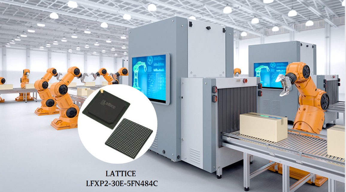
The LATTICE LFXP2-30E-5FN484C is a Field-Programmable Gate Array (FPGA) based on the flexiFLASH architecture of the LatticeXP2 series. It adopts a 90nm process and has a core power supply voltage of 1.2V. With 29,000 logic units, it is rich in logic resources. Internally, it integrates 7 sysDSP blocks and 28 18x18 multipliers, enabling it to efficiently complete complex digital signal processing tasks. It has 387Kbits of sysMEM EBR embedded block RAM and 56Kbits of distributed RAM, meeting various data storage requirements. This chip supports multiple I/O interface standards, such as LVCMOS, SSTL, HSTL, etc., and has as many as 363 I/O terminals. At the same time, it integrates 4 analog PLLs for clock management. These features make it perform excellently in scenarios such as digital signal processing, data storage and transmission, and can provide reliable solutions for developers.
LATTICE LFXP2-30E-5FN484C's Features
Architecture Features
- flexiFLASH Architecture: It features instant-on startup, infinite reconfigurability, a single-chip design, and integrates FlashBAK technology and serial TAG memory to ensure design security.
- Logic and Storage Resources: It contains Look-Up Table (LUT)-based logic blocks (PFU and PFF) that can implement various logic, arithmetic, and storage functions. With up to 387Kbits of sysMEM™ EBR embedded block RAM and 56Kbits of distributed RAM, it provides ample space for data storage.
- Clock Management: Equipped with up to 4 analog PLLs (sysCLOCK PLLs), it can perform clock multiplication, division, and phase-shifting functions to meet the clock requirements of different modules.
- I/O Features: The flexible sysIO buffers support multiple I/O standards such as LVCMOS, SSTL, HSTL, etc., facilitating interfacing with different external devices. Additionally, pre-designed source-synchronous interfaces, like the DDR / DDR2 interface with a maximum speed of 200MHz and the 7:1 LVDS interface for display applications, enhance its application capabilities in high-speed data transmission scenarios.
Functional Module Features
- sysDSP Blocks: The device contains 7 sysDSP blocks that support high-performance multiply-accumulate operations. With 28 18x18 multipliers, each block can be flexibly configured to support various data processing functions such as MULT, MAC, MULTADDSUB, MULTADDSUBSUM, etc., making it suitable for digital signal processing applications.
- Configuration and Security Features: It supports SPI (master/slave mode) boot flash interfaces and dual-boot images, enhancing system reliability and flexibility. Embedded Soft Error Detection (SED) macros can perform CRC checks on configuration data and SRAM to promptly detect and handle soft errors.
- Live Update Technology: Integrated with TransFR™ technology, it supports secure updates with 128-bit AES encryption, ensuring the security of designs during field updates. The dual-boot function, combined with an external SPI, enables remote updates during system operation. If there are issues with the new image, it can roll back to the original backup configuration, reducing system risks.
Electrical and Performance Features
- Power Supply and Voltage: The core voltage is 1.2V, and it supports multiple power supplies such as VCC, VCCAUX, VCCPLL, VCCIO, etc. Each power supply has a corresponding recommended operating voltage range to ensure the stable operation of the device.
- DC and Switching Characteristics: Detailed DC and switching characteristic parameters, including absolute maximum ratings, recommended operating conditions, various electrical characteristics (such as input/output leakage current, supply current, etc.), and rich timing parameters (such as clock-to-output delay, setup time, hold time, etc.), provide precise references for circuit design.
- Temperature and Storage: The operating temperature range varies according to different grades, with the commercial grade being 0 - 85°C, the industrial grade being -40 - 100°C, and the storage temperature range being -65 - 150°C, meeting the usage requirements in different environments.
LATTICE LFXP2-30E-5FN484C's Applications
In the field of digital signal processing: This chip has 7 sysDSP blocks and 28 18x18 multipliers, supporting high-performance multiply-accumulate operations, and is suitable for complex digital signal processing tasks. In communication systems, it can be used to implement functions such as Fast Fourier Transform (FFT), Finite Impulse Response (FIR) filtering, Reed-Solomon encoding and decoding, etc., improving the speed and accuracy of signal processing and ensuring communication quality. In audio processing devices, it can perform real-time processing of audio signals, such as noise reduction, mixing, sound effect enhancement, etc., meeting users' needs for high-quality audio.
In storage and data processing systems: The chip integrates up to 387Kbits of sysMEM EBR and 56Kbits of distributed RAM, which can be used as high-speed cache or data storage units. In data acquisition systems, it can quickly store the collected data for subsequent analysis and processing. In embedded systems, it provides high-speed data storage and reading services for microprocessors, optimizing the system's data processing flow and improving the overall operation efficiency.
In communication interfaces and high-speed data transmission: It supports a variety of high-speed interface standards, such as DDR / DDR2 interfaces with a maximum speed of up to 200MHz, and 7:1 LVDS interfaces for display applications. In network devices, it can achieve high-speed data transmission, such as the application of the XGMII standard for Ethernet interfaces, meeting the demand for rapid network data exchange. In display systems, the LVDS interface is used to achieve stable transmission of high-resolution display data, ensuring clear and smooth image display.
In industrial control and automation: It has rich I/O resources and flexible configuration capabilities, supporting a variety of I/O standards, such as LVCMOS, SSTL, HSTL, etc. In industrial automation production lines, it can be used to control various devices, such as motor drive, sensor data acquisition and processing, etc. In intelligent factory systems, it enables efficient communication and collaborative work between devices, enhancing the automation and intelligence level of the production process.
In security and encryption applications: It supports secure updates with 128-bit AES encryption, as well as dual-boot functionality. In secure communication devices, it encrypts the transmitted data to prevent data from being stolen or tampered with, ensuring communication security. In systems with high security requirements, such as financial devices and military communication devices, the dual-boot function and encryption technology are utilized to ensure that the system can quickly recover and operate continuously and securely in case of failures or attacks.
LATTICE LFXP2-30E-5FN484C's Attributes
-
| Product Attribute |
Attribute Value |
| Manufacturer: |
Lattice |
| Product Category: |
FPGA - Field Programmable Gate Array |
| RoHS: |
Y |
| Product: |
XP2 |
| Number of Logic Elements: |
29000 |
| Number of Logic Array Blocks - LABS: |
3625 |
| Number of I/Os: |
363 I/O |
| Operating Supply Voltage: |
1.2 V |
| Minimum Operating Temperature: |
0 C |
| Maximum Operating Temperature: |
+ 85 C |
| Mounting Style: |
SMD/SMT |
| Package / Case: |
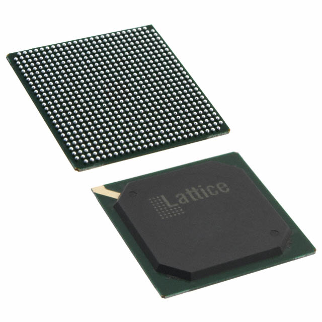
FPBGA-484 |
| Packaging: |
Tray |
| Height: |
1.65 mm |
| Length: |
23 mm |
| Series: |
LFXP2 |
| Width: |
23 mm |
| Brand: |
Lattice |
| Distributed RAM: |
56 kbit |
| Embedded Block RAM - EBR: |
387 kbit |
| Moisture Sensitive: |
Yes |
| Product Type: |
FPGA - Field Programmable Gate Array |
| Factory Pack Quantity: |
60 |
| Subcategory: |
Programmable Logic ICs |
| Supply Voltage - Max: |
1.26 V |
| Supply Voltage - Min: |
1.14 V |
| Total Memory: |
443 kbit |
| Unit Weight: |
0.077955 oz |
| Tags: |
LFXP2-30E-5FN, LFXP2-30E-5, LFXP2-3, LFXP2, LFX |

LATTICE LFXP2-30E-5FN484C's Category-FPGA
FPGA (Field-Programmable Gate Array) is an integrated circuit that can be programmed and configured through a hardware description language. It adopts a structure of logic cell arrays and contains abundant logic resources, storage units, clock management modules, and various I/O interfaces. Thanks to its flexible reconfigurability, FPGA can quickly adapt to different application requirements and is widely applied in fields such as communication, digital signal processing, artificial intelligence, and industrial control. In 5G communication, FPGA can achieve high-speed data modulation and demodulation; in the field of artificial intelligence, it is used to accelerate neural network computing.
As a member of the FPGA family, the LATTICE LFXP2-30E-5FN484C is based on the flexiFLASH architecture of the LatticeXP2 series, possessing both instant startup and infinite reconfigurability features. With its rich sysDSP blocks, multipliers, RAM resources, and diverse I/O interface standards, it performs outstandingly in application scenarios such as digital signal processing, data storage, and transmission. It can provide developers with efficient and reliable solutions, helping to achieve complex functional requirements.
LFXP2-30E-5FN484C's Manufacturer-LATTICE
LATTICE has made remarkable achievements in the field of FPGA (Field - Programmable Gate Array). As the company with the largest FPGA shipments globally, it serves over 10,000 customers. In the past decade, about 5 billion FPGA devices have been sold worldwide, and the demand is expected to reach 10 billion units in the next ten years. LATTICE occupies an important position by virtue of its own advantages. LATTICE has been deeply engaged in the field of low-power FPGA for over 40 years and has achieved fruitful results. Its launched products such as the Nexus series, compared with competitors, have up to 4 times lower power consumption, 2 times higher video connection performance, and only one-tenth of the size of competitors. The Nexus 2 platform released in 2024, with enhanced connectivity, optimized power consumption and performance, as well as leading security and reliability, won the 2025 BIG Innovation Award. In the mid-range market, the Avant series of FPGAs, compared with the Nexus platform released seven years ago, has seen a 5-fold increase in logical resources, a 10-fold increase in connection bandwidth, and a 30-fold increase in system performance, providing customers with more choices. In terms of technological innovation, LATTICE keeps making breakthroughs. For example, the Avant FPGA adopts technologies such as early I/O enablement, ultra-high-speed configuration interfaces, bitstream compression, and TransFR, breaking the limitations of startup time and being 10 times faster than its counterparts in startup speed. In the emerging field of AI, LATTICE has made early arrangements. It acquired the AI software company Mirametrix in 2021, and its revenue in the AI field exceeded 100 million US dollars in 2023. It continues to develop related applications and promotes the application and development of FPGA in the AI field.
Specification Comparison: LFXP2-30E-6F672C vs LFXP2-30E-6FN672I vs LFXP2-30E-5FN484C
Pictures
Part Number |
|

|
|
| Manufacturer |
Lattice Semiconductor Corporation |
Lattice Semiconductor |
Lattice Semiconductor |
| Package |
672-BBGA |
FPBGA-672 |
FPBGA-484 |
| Description |
Highly efficient logic processing
for high-speed application |
Low-power, high-density field-programmable
gate array solution |
Advanced logic features with I/O
interfaces for efficient contro |
| Stock |
7904 |
4879 |
4138 |
| Series |
XP2 |
LFXP2 |
LFXP2 |
| Package / Case |
672-BBGA |
FPBGA-672 |
FPBGA-484 |
| Product Category |
|
FPGA - Field Programmable Gate Array |
FPGA - Field Programmable Gate Array |
| RoHS |
|
Details |
Details |
| Number of Logic Elements |
|
29000 LE |
29000 LE |
| Adaptive Logic Modules - ALMs |
|
14500 ALM |
14500 ALM |
| Embedded Memory |
|
387 kbit |
387 kbit |
| Number of I/Os |
|
472 I/O |
363 I/O |
| Supply Voltage - Min |
|
1.14 V |
1.14 V |
| Supply Voltage - Max |
|
1.26 V |
1.26 V |
| Minimum Operating Temperature |
|
- 40 C |
0 C |
| Maximum Operating Temperature |
|
+ 100 C |
+ 85 C |
| Mounting Style |
|
SMD/SMT |
SMD/SMT |
| Brand |
|
Lattice |
Lattice |
| Maximum Operating Frequency |
|
357 MHz |
311 MHz |
| Moisture Sensitive |
|
Yes |
Yes |
| Number of Logic Array Blocks - LABs |
|
3625 LAB |
3625 LAB |
| Product Type |
|
FPGA - Field Programmable Gate Array |
FPGA - Field Programmable Gate Array |
| Factory Pack Quantity |
|
40 |
60 |
| Subcategory |
|
Programmable Logic ICs |
Programmable Logic ICs |
| Distributed RAM |
|
|
56 kbit |
| Embedded Block RAM - EBR |
|
|
387 kbit |
| Height |
|
|
1.65 mm |
| Length |
|
|
23 mm |
| Operating Supply Voltage |
|
|
1.2 V |
| Total Memory |
|
|
443 kbit |
| Width |
|
|
23 mm |
| Unit Weight |
|
|
0.077955 oz |
| Product Status |
Obsolete |
|
|
| Programmable |
Not Verified |
|
|
| Number of LABs/CLBs |
3625 |
|
|
| Number of Logic Elements/Cells |
29000 |
|
|
| Total RAM Bits |
396288 |
|
|
| Number of I/O |
472 |
|
|
| Voltage - Supply |
1.14V ~ 1.26V |
|
|
| Mounting Type |
Surface Mount |
|
|
| Operating Temperature |
0°C ~ 85°C (TJ) |
|
|
| Supplier Device Package |
672-FPBGA (27x27) |
|
|
| Base Product Number |
LFXP2-30 |
|
WlS Electronic has a vast inventory of LFXP2-30E-5FN484C LATTICE. We guarantee that these are authentic and brand - new components sourced directly from LATTICE. If required, we can provide quality test reports for the LFXP2-30E-5FN484C. To get a quotation, simply fill in the desired quantity, your contact name, and your email address in the quick quotation form on the right - hand side. Our sales representatives will reach out to you within 12 hours. You can contact us online at any time. Moreover, you may send us an email at: SALES@WLSCHIP.COM.


