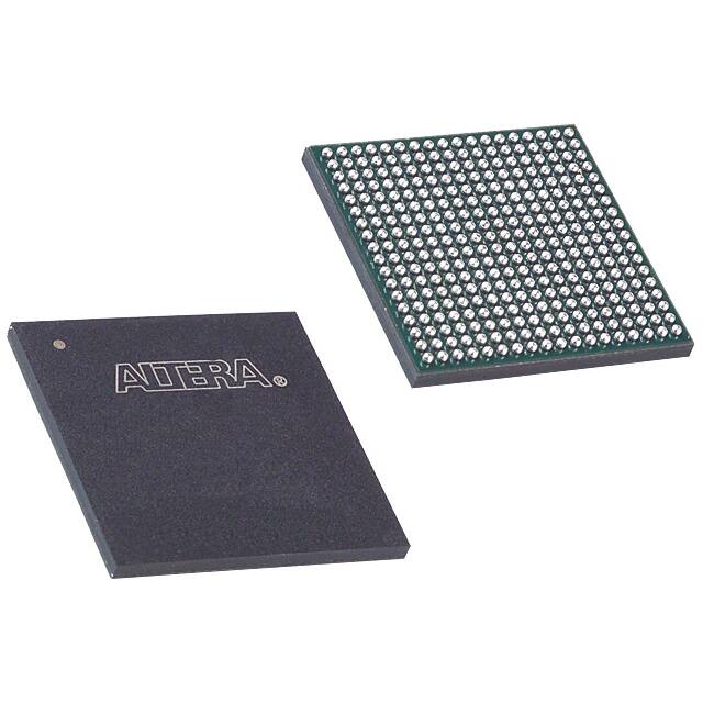
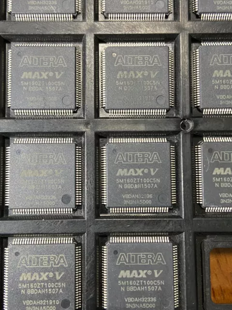
The Intel/Altera 5M160ZT100C5N is a 100 - pin TQFP packaged CPLD. It has 160 logic elements, rich I/O resources with 79 user I/O pins supporting various standards. It features internal oscillator, user flash memory block, and is suitable for low - power, small - size designs, playing a key role in different electronic systems for digital logic control.
Intel / Altera 5M160ZT100C5N's Features
Basic Characteristics: Based on a low-cost, low-power, and non-volatile CPLD architecture, the configuration time is extremely short, only 0.5ms or less, enabling instant startup. The standby current is as low as 25µA, and it has functions of fast power-down and reset operations, effectively reducing system power consumption and meeting the requirements of applications with strict power consumption demands. It supports multiple voltage standards. The internal core is externally powered at 1.8V, and the MultiVolt I/O interface can support logic levels of 3.3V, 2.5V, 1.8V, 1.5V, and 1.2V, facilitating connection and communication with external devices of different voltages.
Performance Characteristics: It has fast propagation delay and clock-to-output time, meeting the needs of digital logic design with high timing requirements. An internal oscillator is integrated to provide a clock signal for the chip, reducing the need for an external clock source and lowering system cost and complexity. It supports simulated RSDS output with a data rate of up to 200Mbps and simulated LVDS output with a data rate of up to 304Mbps, making it suitable for applications requiring high-speed data transmission. It has four global clocks, and each Logic Array Block (LAB) can use two of them, providing stable clock signals for various logic resources within the chip to ensure synchronous operation of the system.
Resource Characteristics: With a density of 160 Logic Elements (LEs), it can provide abundant logic resources for implementing various complex digital logic functions. It includes user flash memory blocks with a capacity of up to 8Kbits, which can be used for non-volatile storage and support up to 1000 read and write cycles, facilitating the storage of configuration information, user data, etc. It supports multiple memory types, such as FIFO synchronous read and write, FIFO asynchronous read and write, 1-port SRAM, 2-port SRAM, 3-port SRAM, and shift registers, meeting the storage function requirements of different applications.
I/O Characteristics: It has rich I/O resources, with 79 user I/O pins in the 100-pin TQFP package, enabling flexible connection to external devices. The I/O pins have multiple functions, such as supporting various I/O standards (LVTTL, LVCMOS, LVDS, RSDS, etc.), complying with the 3.3V, 32-bit, 33MHz PCI specification, supporting JTAG boundary scan testing, and having programmable drive strength control, weak pull-up resistors, slew rate control, tri-state buffers, bus hold circuits, programmable pull-up resistors, open-drain outputs, Schmitt trigger inputs, fast I/O connections, and programmable input delay functions, meeting the diverse requirements of I/O interfaces in different application scenarios.
Other Characteristics: It adopts a space-saving package form, such as the 100-pin TQFP package, which is convenient for layout on the circuit board. It supports vertical migration, allowing migration to other device models within the same package, facilitating product upgrades and design changes.
Intel / Altera 5M160ZT100C5N's Applications
I/O Expansion: This chip has abundant I/O resources, with 79 user I/O pins in the 100-pin TQFP package. It supports multiple I/O standards, such as LVTTL, LVCMOS, LVDS, RSDS, etc., and its MultiVolt I/O interface can adapt to logic levels of 3.3V, 2.5V, 1.8V, 1.5V, and 1.2V. This makes it perform outstandingly in systems that require an expansion of the number and types of I/O interfaces. For example, in the industrial control field, it can connect to various devices like sensors and actuators to achieve complex control functions. In communication devices, it can meet the requirements of different interface standards, enhancing the device's compatibility.
Bus and Protocol Bridging: In the aspect of bus and protocol bridging, the 5M160ZT100C5N can serve as a conversion bridge between different buses or protocols. It supports the 3.3V, 32-bit, 33MHz PCI specification and can perform data transmission and protocol conversion between the PCI bus and other buses. For example, inside a computer, it assists in efficient communication between different bus devices, ensuring accurate data transmission and enhancing the overall system performance.
Power Monitoring and Control: Relying on its rich internal logic resources and configurable features, the 5M160ZT100C5N can implement complex power monitoring and control algorithms. It can monitor various parameters of the power supply in real-time, such as voltage and current, and perform precise control according to preset conditions. In a server power management system, it monitors and regulates multiple power modules to ensure stable power output and improve the system's reliability and stability.
FPGA Configuration: Regarding FPGA configuration, this chip can be used to store and transfer FPGA configuration data. Its internal user flash memory block can save the FPGA's configuration information. When the system boots up, it accurately transfers the configuration data to the FPGA to ensure the normal operation of the FPGA. This plays a crucial role in application scenarios where FPGA configuration needs to be frequently updated, such as the upgrade and transformation of communication base stations, enabling convenient and fast FPGA configuration updates.
Analog IC Interface: The 5M160ZT100C5N can provide an efficient interface between analog ICs and digital systems. It supports multiple I/O standards and can be connected to different types of analog ICs. In a data acquisition system, it seamlessly interfaces with analog sensors and ADCs, converts analog signals into digital signals, and conducts subsequent processing, enabling effective communication between the analog and digital worlds.

Intel / Altera 5M160ZT100C5N's Attributes
| EU RoHS |
Compliant |
| ECCN (US) |
EAR99 |
| Part Status |
Active |
| HTS |
COMPONENTS |
| Family Name |
MAX® V |
| Logic Elements |
160 |
| Program Memory Type |
Flash |
| Memory Size (Kbit) |
8 |
| Number of Logic Blocks/Elements |
8 |
| Number of Global Clocks |
4 |
| Number of I/O Banks |
2 |
| Number of Macro Cells |
128 |
| Data Gate |
No |
| Maximum Number of User I/Os |
79 |
| In-System Programmability |
Yes |
| Programmability |
Yes |
| Reprogrammability Support |
Yes |
| Programmable Type |
In System Programmable |
| Maximum Internal Frequency (MHz) |
1474.9 |
| Maximum Clock to Output Delay (ns) |
8.6 |
| Maximum Propagation Delay Time (ns) |
14|8.5 |
| Speed Grade |
5 |
| Individual Output Enable Control |
Yes |
| Minimum Operating Supply Voltage (V) |
1.71 |
| Maximum Operating Supply Voltage (V) |
1.89 |
| Typical Operating Supply Voltage (V) |
1.8 |
| I/O Voltage (V) |
1.2|1.5|1.8|2.5|3.3 |
| Tolerant Configuration Interface Voltage (V) |
5 |
| Minimum Operating Temperature (°C) |
0 |
| Maximum Operating Temperature (°C) |
85 |
| Supplier Temperature Grade |
Commercial |
| Packaging |
Tray |
| Tradename |
MAX |

Intel / Altera 5M160ZT100C5N's Symbol, Footprint and 3D Model
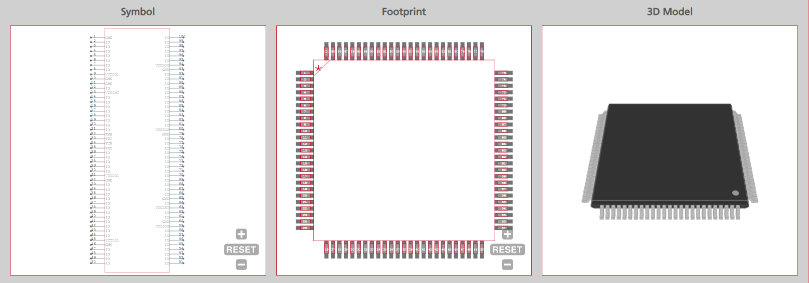
The Intel/Altera 5M160ZT100C5N is a CPLD chip packaged in a 100-pin TQFP. Its pins have diverse functions, covering power supply, I/O, clock, configuration, and other aspects, playing a crucial role in different application scenarios.
Power Supply Pins
- VCCINT: This pin supplies 1.8V power for the internal logic of the chip and in-system programming (ISP). It is a key power input to ensure the normal operation of the internal core functions of the chip, directly powering internal logic units, registers, etc., to ensure their stable operation.
- VCCIO: It is used to power the I/O buffers. Its voltage value varies according to different I/O standards, supporting multiple voltages such as 3.3V, 2.5V, 1.8V, 1.5V, and 1.2V to adapt to the interface requirements of different external devices.
- GND: The ground pin provides an electrical reference ground for the chip, ensuring the electrical stability of the circuit and reducing the impact of electrical noise and interference on the normal operation of the chip.
I/O Pins
With a 100-pin TQFP package, this chip has 79 user I/O pins, featuring a strong interface expansion capability. These pins support multiple I/O standards such as LVTTL, LVCMOS, LVDS, and RSDS, enabling communication with different types of external devices. For example, in the industrial control field, they can be connected to sensors, actuators, etc.; in communication devices, they can meet the requirements of different interface standards. At the same time, the pins also have multiple functional features. For instance, the programmable drive strength control can adjust the output current intensity according to actual needs, enhancing the signal transmission ability; and the support for Schmitt trigger inputs can effectively improve the anti-noise ability of input signals, ensuring stable and reliable signals.
Clock Pins
- GCLK[3..0]: The chip has four dual-purpose dedicated clock pins that can be used to drive the global clock network, providing clock signals for the logic array blocks (LABs), logic elements (LEs), I/O units, etc. inside the chip to ensure the synchronous operation of various circuit parts. If not used for clock functions, these pins can also be used as general-purpose I/O (GPIO), enhancing the flexibility of the pins.
- Pins related to the internal oscillator: The internal oscillator of the chip provides a clock for some of its own operations. Although the document does not clearly mention the specific related pins, the clock signal of the oscillator may be distributed inside the chip through specific pins or output for external use in some cases.
Configuration Pins
- JTAG Pins: They include TMS (Test Mode Select), TCK (Test Clock), TDI (Test Data In), and TDO (Test Data Out), following the IEEE Std. 1149.1 - 1990 standard and are used for the testing, programming, and debugging of the chip. Through the JTAG interface, the configuration of the internal logic of the chip, the input of test vectors, and the output of test results can be achieved, facilitating chip development and verification by developers.
- Other configuration - related pins: When the configuration flash memory block (CFM) and user flash memory block (UFM) inside the chip perform configuration and data read/write operations, specific pins may be required to transmit control signals and data. For example, the programming, erasing, and address and data transmission of the UFM may rely on some dedicated pins. These pins are connected to the logic array to achieve effective control of the memory block and data interaction.
Special Function Pins
- DEV_CLRn: It is a chip-level reset pin that can be used to reset all registers in the chip. Through relevant settings in the Quartus II software, the function of this pin can be controlled. If it is set to the reset function, pulling this signal low before or during chip power - up can prevent the release of clear signals in user mode, thereby achieving precise control of chip reset; if it is not set to the reset function, it can be used as a regular I/O pin.
- DEV_OE: It is a chip-level output enable pin used to control the output states of all output pins on the chip. After setting the function of this pin in the Quartus II software, when DEV_OE is active, all output pins work normally; when DEV_OE is inactive, all output pins enter the tri - state, facilitating the unified control and management of outputs in the system.
Intel / Altera 5M160ZT100C5N's Category-CPLDs
Complex Programmable Logic Devices (CPLDs) are highly integrated digital logic chips that play an important role in modern electronic systems. Composed of multiple logic blocks, interconnection resources, and I/O units, CPLDs possess abundant logic resources and flexible programmable features. CPLDs are capable of implementing various complex digital logic functions, such as the design of combinational logic and sequential logic circuits, and are widely applied in many fields, including communication, industrial control, automotive electronics, and more. Their advantages lie in repeatable programming, which can meet the requirements of different projects, reducing the cost of hardware design and the development cycle. With fast processing speed and good stability, CPLDs can ensure the reliable operation of the system.
The Intel/Altera 5M160ZT100C5N is a typical product among CPLDs and belongs to the MAX V series. It has 160 logic elements and rich I/O resources, with 79 user I/O pins in the 100-pin TQFP package. It supports multiple I/O standards, such as LVTTL and LVCMOS, and the MultiVolt I/O interface can adapt to different voltage logic levels. It also integrates functional modules such as an internal oscillator and user flash memory blocks, effectively meeting the design requirements of low power consumption, small size, and diverse functions, playing a key role in various electronic devices and facilitating the implementation of complex digital logic control.
5M160ZT100C5N's Manufacturer-Intel / Altera
Intel/Altera has achieved remarkable success in the field of CPLDs. Since entering this field, it has continuously introduced innovative products. It has a rich series of CPLD products. For example, the MAX 7000 series, based on eeprom technology, features high density, in-system programmability, and high-speed propagation delay, making it suitable for complex logic scenarios. The MAX II series employs non-volatile flash memory technology, offering high performance and low standby current. The MAX V series integrates multiple technologies to achieve low power consumption and also provides a rich set of functional options. In terms of technology, Intel/Altera has achieved extremely low configuration time. Some products can complete configuration within 0.5ms or even shorter, enabling instant startup. It supports multiple voltage standards and flexibly adapts the internal core to the voltage of external interfaces. Its products are widely used in various fields such as industrial control, communication, and automotive, helping different industries achieve efficient and reliable digital logic control and driving the digitalization process of industries.
5M1270ZF324I5N vs 5M160ZT100C5N
| Pictures |
 |
 |
| Parts |
5M1270ZF324I5N +BOM |
5M160ZT100C5N +BOM |
| Manufacturer |
Altera Corporation (Intel) |
Altera Corporation (Intel) |
| Package |
FBGA - 324 |
TQFP - 100 |
| Description |
5M1270ZF324I5N YES 324 - LBGA 2003 5M1270
complex programmable logic device 201.
1MHz 19mm 6.2ns 1.81.2/3.3V Featuring
5M160ZT100C5N, a CPLD MAX V Flash
128 Cells product with 79 I/O and 160 Labs, delivers a quick 7 |
5M160ZT100C5N, a CPLD MAX V Flash 128 Cells
product with 79 I/O and 160 Labs, delivers a quick 7 |
| Stock |
1806 |
2103 |
| RoHS |
True |
True |
| Series |
5M1270Z |
5M160Z |
| Mounting Style |
SMD/SMT |
SMD/SMT |
| Collector - Emitter Saturation Voltage |
1.8 V |
1.8 V |
| Number of Macrocells |
980 Macrocell |
128 Macrocell |
| Number of GPIO |
271 I/O |
79 I/O |
| Max Supply Voltage |
1.89 V |
1.89 V |
| Supply Voltage - Min |
1.71 V |
1.71 V |
| Minimum Operating Temperature (°C) |
- 40 |
0 |
| Maximum Operating Temperature (°C) |
+ 85 |
+ 85 |
| Maximum Operating Frequency |
304 MHz |
152 MHz |
| Propagation Delay - Max |
6.2 ns |
7.5 ns |
| Memory Type |
Flash |
Flash |
| Moisture Sensitive |
Yes |
Yes |
| Number of Logic Array Blocks - LABs |
127 |
16 |
| Current @ Pmpp |
2 mA |
25 uA |
| Product Type |
CPLD - Complex Programmable Logic Devices |
CPLD - Complex Programmable Logic Devices |
| Factory Pack Quantity |
84 |
90 |
| Total Memory |
8192 bit |
8192 bit |
| Tradename |
MAX V |
MAX V |
| Orderable part number |
968258 |
969128 |
| Unit Weight |
|
0.705479 oz |
WlS Electronic has a vast inventory of Intel / Altera 5M160ZT100C5N. We guarantee that these are authentic and brand - new components sourced directly from Intel / Altera. If required, we can provide quality test reports for the 5M160ZT100C5N. To get a quotation, simply fill in the desired quantity, your contact name, and your email address in the quick quotation form on the right - hand side. Our sales representatives will reach out to you within 12 hours. You can contact us online at any time. Moreover, you may send us an email at: SALES@WLSCHIP.COM.


