In the realm of semiconductor electronics, few components are as foundational yet misunderstood as NPN and PNP transistors. These bipolar junction transistors (BJTs) form the backbone of countless circuits, from simple switches in microcontrollers to complex amplifiers in industrial systems. Despite their ubiquitous presence, the fundamental differences between NPN and PNP transistors—from their semiconductor layer arrangements to their operational polarities—often perplex engineers and hobbyists alike. This comprehensive analysis aims to demystify these devices, unraveling the structural principles that dictate their behavior and the application scenarios that demand their unique capabilities. Whether you’re a seasoned designer seeking to refine your component selection or a student mastering the basics, understanding the nuanced differences between NPN and PNP transistors is crucial for creating reliable, efficient electronic systems. Let’s embark on a journey from their atomic-level carrier transport mechanisms to real-world circuit implementations, empowering you to make informed design decisions with confidence.
I. Core Definitions and Structural Differences: The Code of Semiconductor Layers
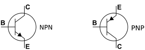
- NPN Transistor: Electron-Driven "Sandwich" Structure
The NPN transistor consists of two N-type semiconductor layers sandwiching a P-type layer (N-P-N structure). The emitter arrow in its symbol points outward, indicating current flow from the emitter. In N-type semiconductors, free electrons are the major charge carriers, while P-type semiconductors rely on holes (positive charge carriers). This structure allows electrons to move from the emitter to the collector when the transistor is conducting, forming the current.
- PNP Transistor: Hole-Driven Mirror Structure
The PNP transistor features two P-type layers sandwiching an N-type layer (P-N-P structure), with the emitter arrow pointing inward to denote current flow into the emitter. It operates with holes as the major carriers, where holes move from the emitter to the collector, with electrons flowing in the opposite direction—forming a mirror-symmetric conduction mechanism to NPN.
Structure Comparison Table:
| Parameter |
NPN Transistor |
PNP Transistor |
| Layer Structure |
N-P-N (N-type outer, P-type inner) |
P-N-P (P-type outer, N-type inner) |
| Emitter Arrow |
Points outward (→) |
Points inward (←) |
| Major Carriers |
Electrons (negative charge) |
Holes (positive charge) |
II. Working Principles: The Two-Way Dance of Polarity and Current
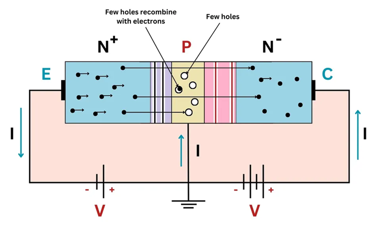
- NPN Transistor: Current Control Under Positive Biasing
- Conduction Condition: When a positive bias (≈0.7V for silicon) is applied to the base (B) relative to the emitter (E), the base-emitter junction (B-E) is forward-biased, and the base-collector junction (B-C) is reverse-biased. Current flows from the collector (C) to the emitter (E).
- Current Relationship: Base current (IB) controls collector current (IC), satisfying IC = β×IB (β is the current gain, typically 50~200).
- Operation Regions:
- Active Region: B-E forward-biased, B-C reverse-biased; IC proportional to IB.
- Cutoff Region: Inadequate base voltage; no current flows.
- Saturation Region: Excessive base voltage; IC is no longer controlled by IB, acting as a closed switch.
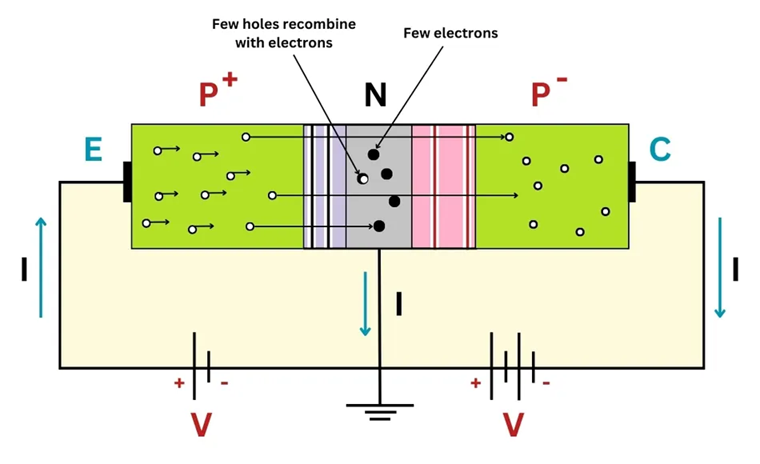
- PNP Transistor: Current Reversal Under Negative Biasing
- Conduction Condition: A negative bias (≈-0.7V for silicon) on the base relative to the emitter forward-biases B-E and reverse-biases B-C, enabling current flow from the emitter to the collector.
- Current Direction: Opposite to NPN; base current exits the transistor, emitter current enters, and collector current exits.
- Key Difference: PNP biasing polarity is entirely opposite to NPN, suitable for negative supply or high-side switching scenarios.
Biasing and Current Direction Comparison:
plaintext
NPN Biasing Example:          PNP Biasing Example:
Vcc(+) ──┬─ Rc ──┬─ C       E ──┬─ Rc ──┬─ Vcc(+)
          │        │          │        │
          └─ B ── Rb ──┬─ Vbb    └─ Rb ──┬─ B
                   │                   │
                   └─ E ── GND          └─ C ── GND
(NPN: Base positive to conduct)  (PNP: Base negative to conduct)
 NPN Transistor Working Principle
 PNP Transistor Working Principle
III. Application Scenarios: From Logic Circuits to Industrial Control
- NPN: The Preferred Choice for Digital Logic and Low-Side Switching
- Digital Circuits: Acts as an MCU output-stage switch (e.g., Arduino driving an LED), conducting at high level to ground the load (low-side switching).
- Sensor Interfaces: NPN proximity sensors output low level when triggered, compatible with sinking input modules.
- High-Frequency Amplification: Faster electron mobility suits RF amplification, PWM signal generation (e.g., 555 timer circuits).
- PNP: The Core of Industrial Control and High-Side Switching
- Industrial Sensors: PNP photoelectric sensors output high level when triggered, compatible with sourcing PLC input modules.
- Motor Drives: Serves as a high-side switch to control the power 端 of motors, pairing with NPN in push-pull circuits (e.g., L298N motor driver).
- Battery-Powered Circuits: Directly controls load connection to the supply in positive-ground systems (e.g., certain automotive circuits).
Typical Application Comparison Table:
| Domain |
NPN Transistor Applications |
PNP Transistor Applications |
| Digital Logic |
MCU IO switching, TTL logic gates |
Complementary output circuits with NPN |
| Motor Control |
Ground-side control (e.g., stepper motors) |
Power-side control (high-side protection) |
| Sensor Systems |
NPN proximity switches (low-level output) |
PNP photoelectric switches (high-level output) |
| Audio Amplification |
Single-ended amplifiers |
Push-Pull amplifiers with NPN (e.g., LM386) |
IV. Load Connection and Logic Polarity: Key Choices in Circuit Design
- NPN: Sinking Load Connection
- Connection: Load connects to Vcc and NPN collector, with emitter grounded.
- Logic Features: Conducts at high base level (e.g., 5V), allowing load current to flow from collector to emitter (ground) — "low-level active".
- Case: In a relay control circuit, NPN base connects to MCU high level; the relay coil connects to 12V and NPN collector, energizing when conducted.
- PNP: Sourcing Load Connection
- Connection: Load connects to PNP emitter and ground, with collector to Vcc.
- Logic Features: Conducts when base is grounded (low level), supplying Vcc to the load — "high-level active".
- Case: A triggered PNP sensor outputs 24V to a PLC input module, indicating activation.
V. Selection Decision Tree: Four Steps to the Optimal Choice
- Step 1: Determine Switching Position
- Low-side switch (controls ground): Choose NPN (load connects to Vcc, transistor to GND).
- High-side switch (controls power): Choose PNP (load connects to GND, transistor to Vcc).
- Step 2: Confirm Logic Signal Polarity
- Positive logic (high level active): Choose PNP (base grounded to conduct).
- Negative logic (low level active): Choose NPN (base positive to conduct).
- Step 3: Match Power Polarity
- Negative-ground system (Vcc positive, GND negative): Prioritize NPN (e.g., 5V MCU systems).
- Positive-ground system (GND positive, Vcc negative): Prioritize PNP (e.g., certain industrial negative supply circuits).
- Step 4: Compatibility with Sensors/PLCs
- NPN sensors (low-level output): Require sinking input modules.
- PNP sensors (high-level output): Require sourcing input modules.
VI. Implicit Rules in Industrial Applications
- Safety Design Considerations
- PNP Sensor Mis-trigger Protection: A damaged PNP sensor wire grounding defaults to "unactivated" (low level), whereas an NPN sensor grounding mis-triggers "activation". Thus, industrial safety systems prefer PNP.
- Regional Standard Differences
- European Industrial Standards: Tend to use PNP sensors (sourcing output) for positive logic compatibility.
- Asian/North American Standards: NPN sensors (sinking output) are more prevalent, aligning with MCU logic.
VII. Common Questions and Misconceptions
- Can NPN and PNP be directly substituted?
- No. Substitution requires adjusting biasing polarity and load connection. For example, replacing NPN with PNP demands reversing the power supply and swapping load connections.
- Why is NPN more common than PNP?
- Faster Electron Mobility: Electrons move 3x faster than holes, making NPN suitable for high-frequency scenarios.
- Lower Manufacturing Cost: N-type semiconductor doping is simpler, reducing mass production costs by ~30% compared to PNP.
- Difference Between NPN vs. PNP
| Feature |
NPN Transistor |
PNP Transistor |
| Semiconductor Layer Structure |
Negative-Positive-Negative (N-P-N) |
Positive-Negative-Positive (P-N-P) |
| Current Direction |
From collector to emitter |
From emitter to collector |
| Base Activation |
Turns ON when a positive voltage/current is applied to the base |
Turns ON when the base is at a lower potential than the emitter (no current or slight negative) |
| Deactivation Condition |
Turns OFF when base current is reduced or removed |
Turns OFF when base becomes more positive or current flows into base |
| Voltage Requirement for Operation |
Requires a positive voltage at the base relative to emitter |
Requires a negative voltage at the base relative to emitter |
| Internal Structure |
P-layer between two N-layers |
N-layer between two P-layers |
| Switching Logic |
Sinking sensor – load is between positive supply and collector |
Sourcing sensor – load is between emitter and negative supply |
| Operation |
Widely used in digital logic circuits and switching |
Used in circuits where default ON state is required |
| Signal Polarity |
Activated by positive logic (positive voltage) |
Activated by negative logic (low or ground) |
| Connection to Load |
Load connected between positive voltage & collector |
Load connected between emitter & negative (ground) |
| Current Flow Initiation |
Collector current flows when base-emitter junction is forward biased |
Emitter current flows when base-emitter junction is forward biased |
VIII. Conclusion: Design Philosophy Beyond Polarity
The essential difference between NPN and PNP lies not only in structure and current direction but also in the "energy control logic" of circuit design:
- NPN represents "positive control of ground", ideal for digital logic and high-speed switching.
- PNP represents "ground control of positive", suitable for industrial signaling and safety systems.
Mastering their core involves understanding the triangle of "carriers-biasing-loads": carriers determine conduction direction, biasing defines conduction conditions, and load position dictates switching type. Whether designing an MCU board or debugging industrial sensors, following this logic ensures precise device selection and avoids circuit failures from polarity errors.
WlS Electronic maintains a substantial inventory of NPN and PNP transistors, featuring popular models such as 2N2222 (NPN) and 2N2907 (PNP). All components are guaranteed genuine and brand-new, sourced directly from leading manufacturers like ON Semiconductor and Nexperia. For quality assurance, we can provide detailed test reports for each transistor model upon request.
Key Models in Stock:
- NPN Transistors:
- 2N2222/2N2222A: 40V/600mA, hFE 110-800, TO-92 package, suitable for general-purpose amplification and switching.
- BC547: 45V/100mA, hFE 110-800, SOT-23/TO-92, ideal for low-power digital logic.
- PNP Transistors:
- 2N2907/2N2907A: 40V/600mA, hFE 100-600, TO-92 package, perfect for complementary amplifiers and high-side switching.
- BC557: 45V/100mA, hFE 110-800, SOT-23/TO-92, suitable for low-voltage analog circuits.
Why Choose Our Transistors?
- Genuine & New: Direct procurement from original manufacturers ensures performance consistency.
- Comprehensive Testing: Every batch undergoes rigorous testing for parameters like hFE, VCE(sat), and reverse leakage.
- Flexible Quantity: Support small-batch prototyping and large-volume production orders.
To request a quotation, simply fill in the quantity, your name, and email in the quick quote form on the right. Our sales team will contact you within 12 hours. For immediate assistance:
- Contact us online via the live chat feature.
- Email us at: SALES@WLSCHIP.COM
Trust WlS Electronic for reliable NPN/PNP transistors that meet your circuit design needs—from hobby projects to industrial applications. 


