
| Parameter | Specification |
|---|---|
| Operating Temperature Range | -40°C to +100°C (industrial grade; extended temperature options available for aerospace use) |
| Speed Grades | Covers -5 (fastest) to -10 (cost-optimized); maximum propagation delay (tPD) as low as 4.5ns |
| Voltage Tolerance | Core voltage (VCC): 3.3V ±5%; I/O voltage (VCCIO): 2.5V/3.3V/5V ±10% |
| Reliability | MTBF (Mean Time Between Failures) > 10^7 hours; ESD protection (HBM) > 2kV |
| EMI Compliance | Meets CISPR 22 Class B (radiated emissions); built-in slew rate control reduces noise |


| Part Number | Pin/Ball Spacing | θJA (C/Watt) | θJC (C/Watt) | Package Type | Package Body Dimensions | I/O | Commercial (C) | Industrial (I)(1) |
|---|---|---|---|---|---|---|---|---|
| XC2C256-6VQ100C | 0.5mm | 43.1 | 10.9 | Very Thin Quad Flat Pack | 14mm x 14mm | 80 | C | |
| XC2C256-7VQ100C | 0.5mm | 43.1 | 10.9 | Very Thin Quad Flat Pack | 14mm x 14mm | 80 | C | |
| XC2C256-6CP132C | 0.5mm | 65.0 | 15.0 | Chip Scale Package | 8mm x 8mm | 106 | C | |
| XC2C256-7CP132C | 0.5mm | 65.0 | 15.0 | Chip Scale Package | 8mm x 8mm | 106 | C | |
| XC2C256-6TQ144C | 0.5mm | 37.2 | 7.2 | Thin Quad Flat Pack | 20mm x 20mm | 118 | C | |
| XC2C256-7TQ144C | 0.5mm | 37.2 | 7.2 | Thin Quad Flat Pack | 20mm x 20mm | 118 | C | |
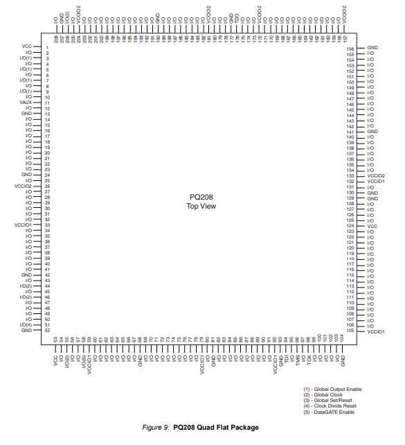
| XC2C256-6PQ208C | 0.5mm | 36.9 | 9.7 | Plastic Quad Flat Pack | 28mm x 28mm | 173 | C | |
| XC2C256-7PQ208C | 0.5mm | 36.9 | 9.7 | Plastic Quad Flat Pack | 28mm x 28mm | 173 | C | |
| XC2C256-6FT256C | 1.0mm | 34.6 | 6.1 | Fine Pitch Thin BGA | 17mm x 17mm | 184 | C | |
| XC2C256-7FT256C | 1.0mm | 34.6 | 6.1 | Fine Pitch Thin BGA | 17mm x 17mm | 184 | C | |
| XC2C256-6VQG100C | 0.5mm | 43.1 | 10.9 | Very Thin Quad Flat Pack; Pb-free | 14mm x 14mm | 80 | C | |
| XC2C256-7VQG100C | 0.5mm | 43.1 | 10.9 | Very Thin Quad Flat Pack; Pb-free | 14mm x 14mm | 80 | C | |
| XC2C256-6CPG132C | 0.5mm | 65.0 | 15.0 | Chip Scale Package; Pb-free | 8mm x 8mm | 106 | C | |
| XC2C256-7CPG132C | 0.5mm | 65.0 | 15.0 | Chip Scale Package; Pb-free | 8mm x 8mm | 106 | C | |
| XC2C256-6TQG144C | 0.5mm | 37.2 | 7.2 | Thin Quad Flat Pack; Pb-free | 20mm x 20mm | 118 | C | |
| XC2C256-7TQG144C | 0.5mm | 37.2 | 7.2 | Thin Quad Flat Pack; Pb-free | 20mm x 20mm | 118 | C | |
| XC2C256-6PQG208C | 0.5mm | 36.9 | 9.7 | Plastic Quad Flat Pack; Pb-free | 28mm x 28mm | 173 | C | |
| XC2C256-7PQG208C | 0.5mm | 36.9 | 9.7 | Plastic Quad Flat Pack; Pb-free | 28mm x 28mm | 173 | C | |
| XC2C256-6FTG256C | 1.0mm | 34.6 | 6.1 | Fine Pitch Thin BGA; Pb-free | 17mm x 17mm | 184 | C | |
| XC2C256-7FTG256C | 1.0mm | 34.6 | 6.1 | Fine Pitch Thin BGA; Pb-free | 17mm x 17mm | 184 | C | |
| XC2C256-7VQ100I | 0.5mm | 43.1 | 10.9 | Very Thin Quad Flat Pack | 14mm x 14mm | 80 | I | |
| XC2C256-7CP132I | 0.5mm | 65.0 | 15.0 | Chip Scale Package | 8mm x 8mm | 106 | I | |
| XC2C256-7TQ144I | 0.5mm | 37.2 | 7.2 | Thin Quad Flat Pack | 20mm x 20mm | 118 | I | |
| XC2C256-7PQ208I | 0.5mm | 36.9 | 9.7 | Plastic Quad Flat Pack | 28mm x 28mm | 173 | I | |
| XC2C256-7FT256I | 1.0mm | 34.6 | 6.1 | Fine Pitch Thin BGA | 17mm x 17mm | 184 | I | |
| XC2C256-7VQG100I | 0.5mm | 43.1 | 10.9 | Very Thin Quad Flat Pack; Pb-free | 14mm x 14mm | 80 | I | |
| XC2C256-7CPG132I | 0.5mm | 65.0 | 15.0 | Chip Scale Package; Pb-free | 8mm x 8mm | 106 | I | |
| XC2C256-7TQG144I | 0.5mm | 37.2 | 7.2 | Thin Quad Flat Pack; Pb-free | 20mm x 20mm | 118 | I | |
| XC2C256-7PQG208I | 0.5mm | 36.9 | 9.7 | Plastic Quad Flat Pack; Pb-free | 28mm x 28mm | 173 | I | |
| XC2C256-7FTG256I | 1.0mm | 34.6 | 6.1 | Fine Pitch Thin BGA; Pb-free | 17mm x 17mm | 184 | I |
